
TFT LCD Red/Blue Mura: Root Cause and Prevention
A TFT LCD red/blue mura case often starts as a practical quality complaint: a local red, blue, or mixed color patch appears on the display, most clearly on a black screen. In many module projects, this is not an interface problem or a software color setting. It is pressure-related optical damage inside the LCD cell.
That distinction matters. If the issue is treated as a driver IC, RGB data, or firmware problem, the team may spend days checking the wrong path. If the symptom changes with data mapping or timing, start with the TFT LCD interface guide. If the mark remains visible as a local optical defect, review the custom TFT LCD module together with glass thickness, cell design, lamination pressure, handling method, and packaging clearance.
Field diagnosis: when red/blue mura is visible even without driving voltage, the first suspect should be mechanical pressure damage. The most common path is glass deformation, photo-spacer movement, PI alignment layer scratch, and local light leakage.
What TFT LCD Red/Blue Mura Looks Like
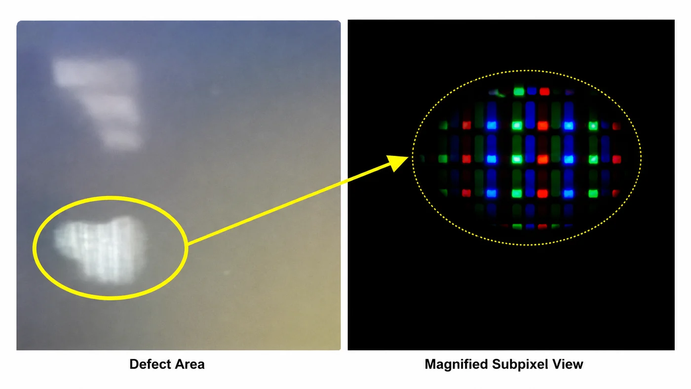
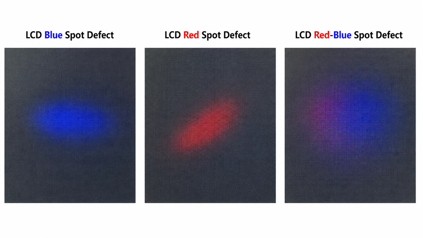
Red/blue mura refers to a local abnormal display area that appears red, blue, or red-blue instead of following the intended image. It may look like an irregular color patch, a soft spot, or a local color shift. The defect is usually easier to see on a black screen because the affected pixels leak light or show abnormal optical behavior.
A practical clue is whether the mark remains visible when the panel is not actively driven. If the abnormal area can still be seen without voltage, the issue is less likely to be a pure signal, timing, or interface fault. The module should be inspected for pressure history, including splitting, handling, bonding, tray design, and vacuum packaging.
How Pressure Creates Color Mura Inside the Cell
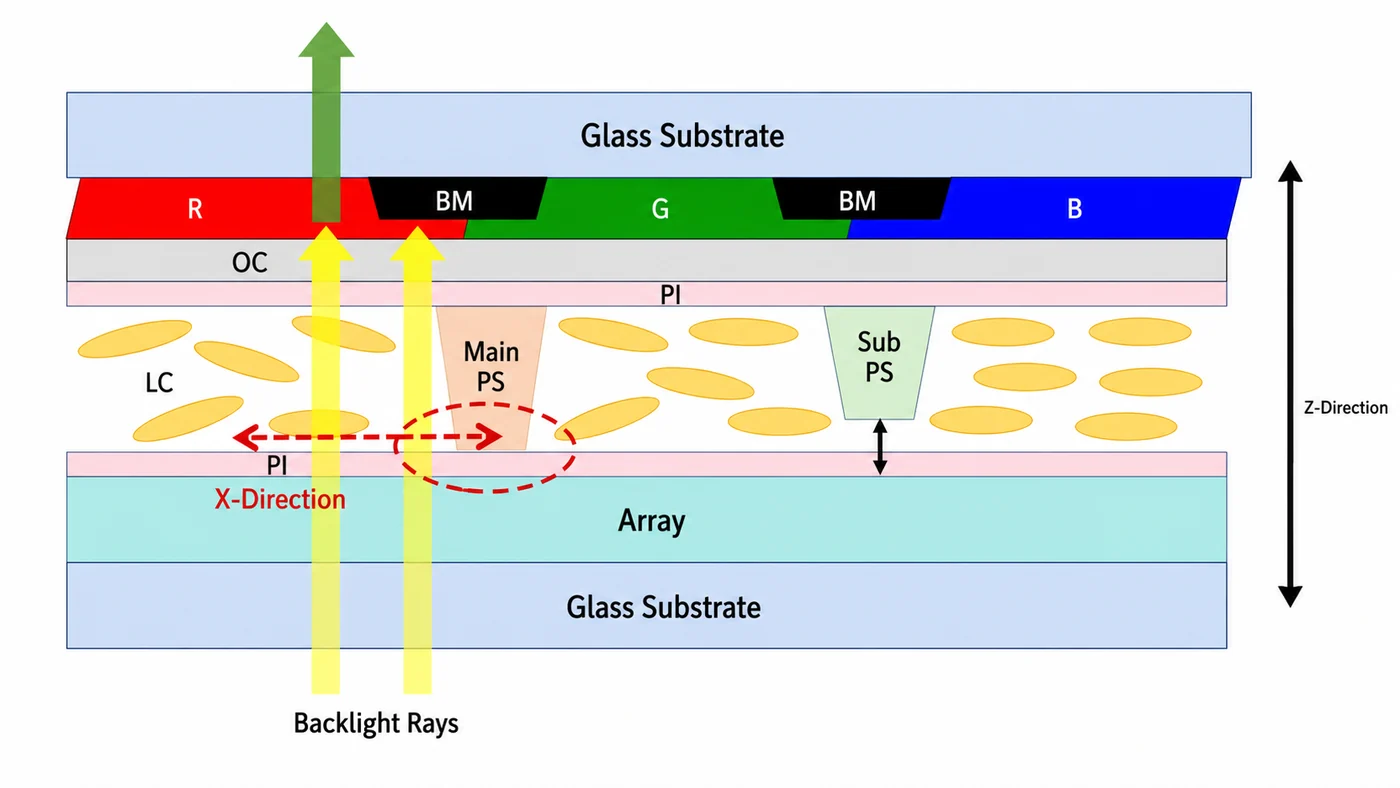
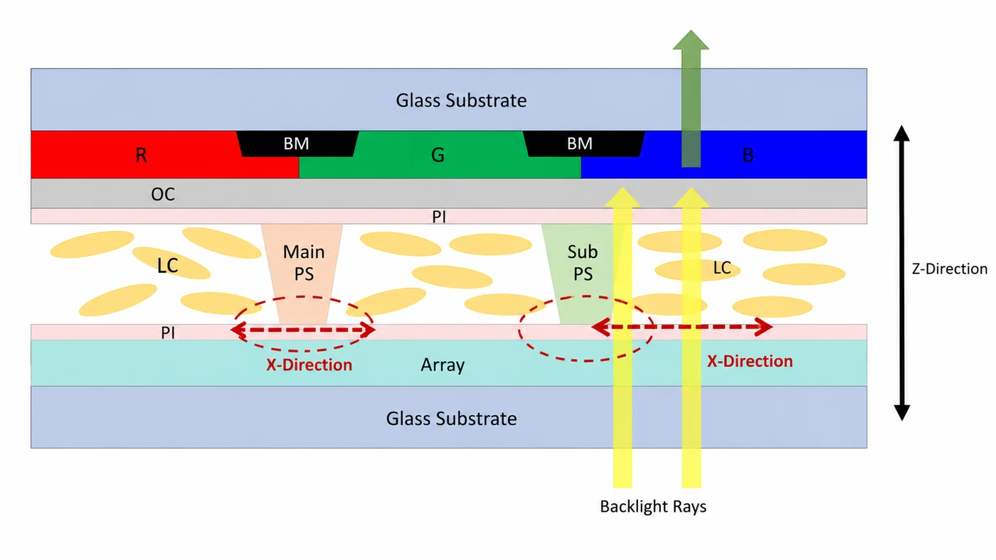
The core mechanism is mechanical. External force bends or compresses the glass substrate. When that force includes both vertical pressure and horizontal sliding, the internal photo spacer can move against the alignment layer. Once the PI alignment layer is scratched, the liquid crystal can no longer align normally in that local area.
In a normally black IPS-type display, damaged alignment can create local light leakage on a black screen. Because each pixel contains red, green, and blue subpixels, a small local alignment failure may be seen as a colored patch rather than a white mark.
Three terms are useful here:
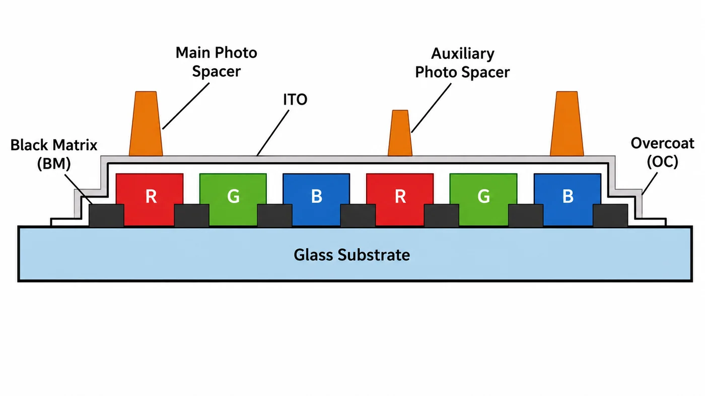
- BM, or black matrix: the opaque area on the color filter side that masks non-emitting or non-display regions.
- PI alignment layer: the polyimide layer that controls the initial liquid-crystal alignment direction.
- Main PS and Sub PS: photo spacers that help maintain cell gap. Main spacers carry more of the gap-support function, while auxiliary spacers provide additional support under larger compression.
Single-Color Mura vs Multi-Color Mura
In failure analysis, it helps to separate single-color mura from multi-color mura. The difference is not only visual. It often points to different pressure severity and different spacer behavior.
Single-color mura: smaller pressure, main spacer movement
When the external force is relatively small, the main photo spacer may be compressed and pushed sideways, while the auxiliary spacer does not yet contact or scratch the PI layer in the same way. The main spacer moves from the protected black matrix area toward an active subpixel area and scratches the PI layer.
The damaged PI area loses its anchoring ability. The local liquid crystal alignment becomes abnormal, and the affected subpixel leaks light. Depending on the spacer movement direction and which subpixel region is exposed, the visible defect may appear red, blue, or another single dominant color.
Multi-color mura: stronger pressure, main and auxiliary spacer scratches
When the pressure increases, the main spacer deformation can exceed the height difference between the main spacer and auxiliary spacer. At that point, both main and auxiliary spacers may scratch the PI layer. The result is no longer a single localized color mark; several subpixel areas can be affected, so the defect appears as mixed red-blue or multi-color mura.
Because auxiliary spacers are usually more numerous than main spacers, severe compression can create more scattered defect points. That is why packaging or handling pressure may produce a broader color-mark pattern instead of one clean spot.
Why Modern TFT LCD Panels Are More Sensitive
Red/blue mura is easier to trigger when the product pushes for thinner glass, larger panel size, higher transmittance, or higher resolution. These improvements are useful for the final device, but they reduce the mechanical margin if the module process is not adjusted at the same time.
| Design or process trend | Why it increases risk | Engineering control |
|---|---|---|
| Larger LCD panel | A larger glass area is easier to press, bend, or twist during transfer, assembly, and inspection. | Use larger handling support areas and avoid point pressure on the active area. |
| Thinner glass | Thin glass has lower resistance to deformation under the same external force. | Keep thinning thickness within a controlled range, especially for high-risk applications. |
| Higher transmittance | Higher aperture/transmittance designs may reduce spacer count or support margin. | Balance transmittance target with spacer density and pressure resistance. |
| Higher resolution | Narrower black matrix width gives less masking margin when the spacer shifts. | Review BM margin and spacer location during panel selection and quality review. |
For more background on the glass, TFT, and color-filter stack, see the TFT-LCD array substrate structure and TFT-LCD array materials articles.
Process Controls That Reduce Red/Blue Mura Risk
Once the mechanism is clear, the prevention logic is straightforward: improve panel pressure resistance where practical, and remove unnecessary pressure from the module process. The risk is not controlled by one station alone. It must be reviewed across the full TFT LCD module manufacturing process.
1. Improve the panel’s pressure resistance
A stronger glass substrate can improve resistance to deformation, but it may increase panel cost. Increasing main and auxiliary spacer density can also improve pressure resistance, but it may reduce optical transmittance. The design target has to balance brightness, transmittance, thickness, strength, and cost.
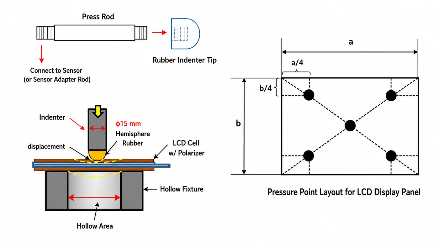
Many projects use an LCD pressure test to screen pressure sensitivity. A common customer-specific target may be, for example, no visible mura, color spot, or light leakage after a defined pressure load such as 60 N. That number should not be treated as a universal rule. The force, indenter, position, duration, judgment image, and acceptance criteria must be written into the customer specification.
2. Control glass thinning thickness
Many TFT and color-filter glass substrates are processed at a thicker state during front-end manufacturing to protect yield, then thinned later for the final module. For phone and tablet panels, single-substrate thickness after thinning is often around 0.15 to 0.25 mm. When the glass becomes too thin, red/blue mura risk increases sharply under handling pressure.
If the device can tolerate it, keeping total LCD thickness near the middle or upper side of the approved range gives better mechanical margin. This is especially relevant for larger displays, handheld devices, and products that require vacuum packaging or optical bonding.
3. Avoid active-area pressure during splitting and handling
During LCD splitting or breaking, operators may press the wrong place if the work instruction is unclear. Pressing the active display area raises the chance of spacer movement and PI damage. The safer method is to press along the cutting line or supported edge area, not the display area.
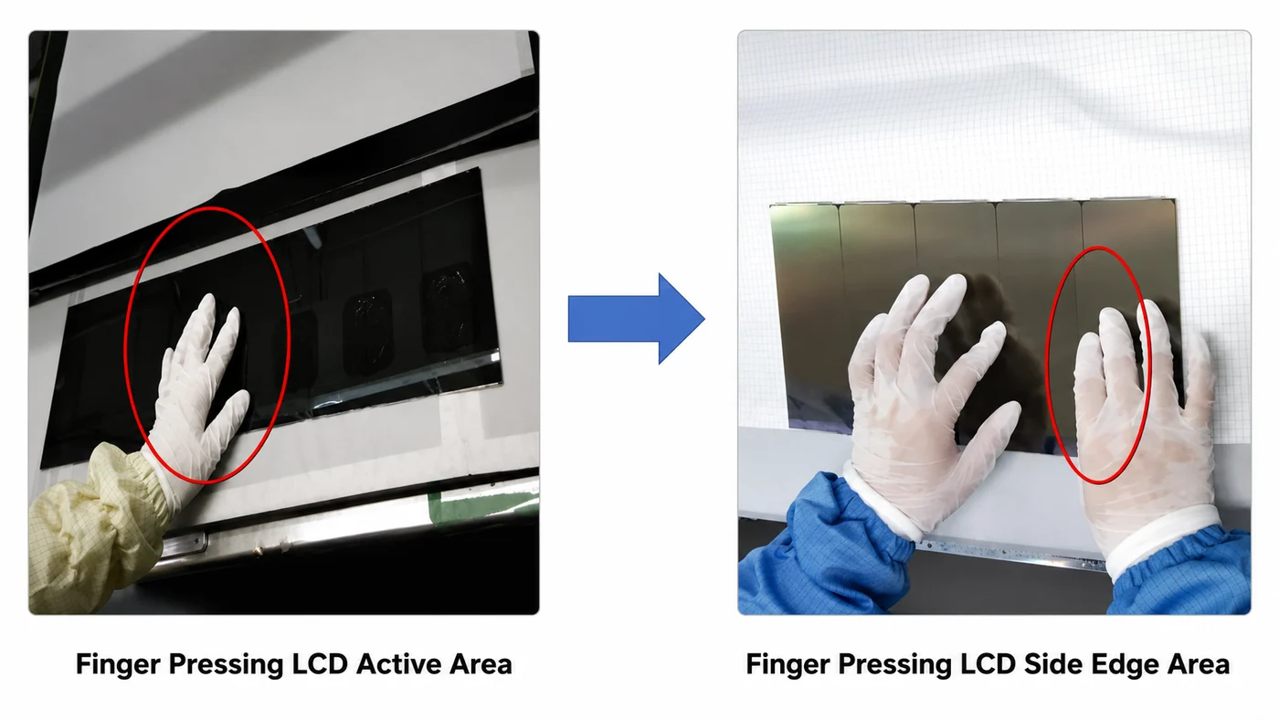
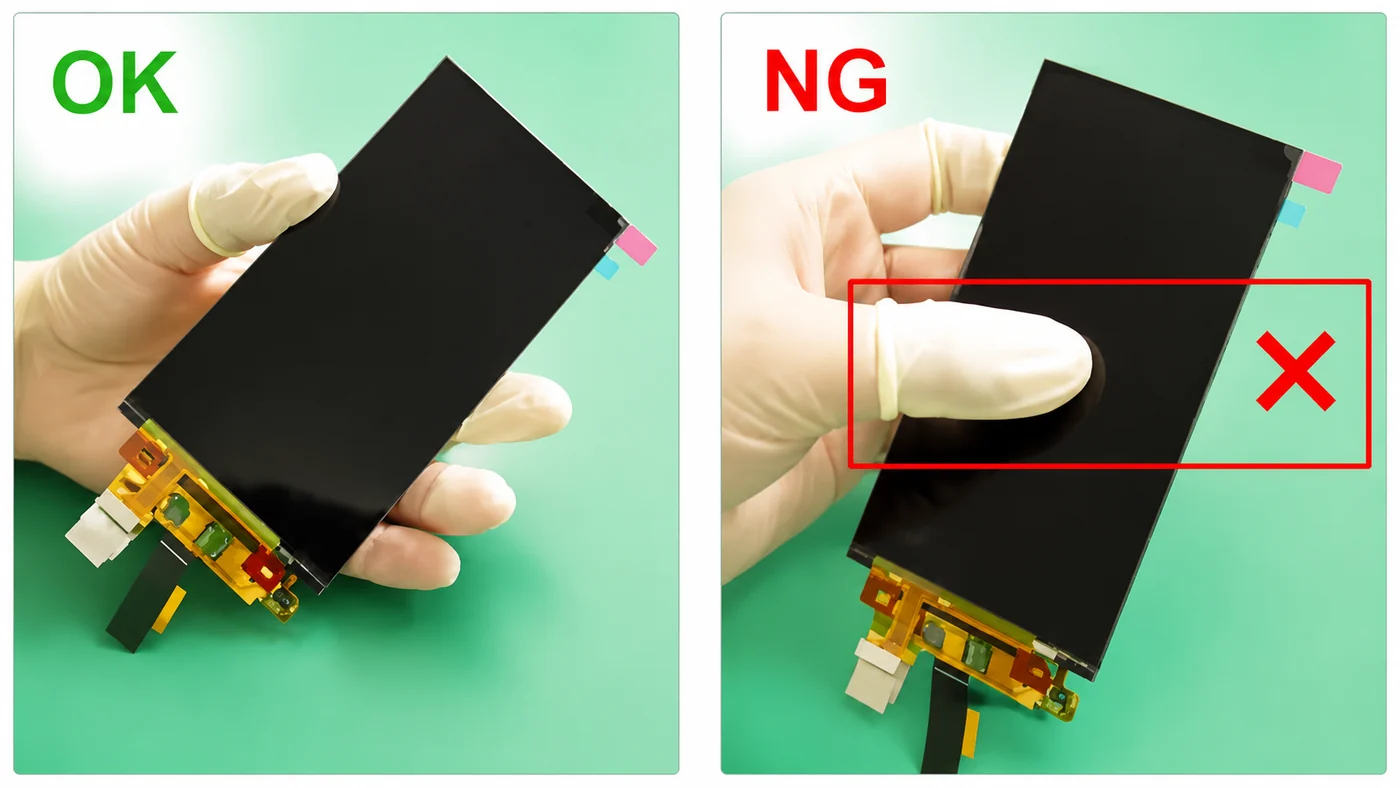
The same logic applies during transfer. Operators should hold the long-side edges of the module and avoid pressing the center display area. It is a simple control, but it is often where pressure damage enters production.
4. Tune lamination and bonding parameters
During film attachment, touch-panel and cover-lens bonding, or hard-to-hard lamination, pressure, insertion amount, speed, vacuum level, bonding time, and platform flatness all matter. A hard particle on the platform can become a local pressure point. For high-resolution or thin-glass panels, this can be enough to create red/blue mura even when the overall bonding pressure looks normal.
Good process control should include platform cleanliness, fixture flatness, pressure distribution, material stack thickness, and post-bonding black-screen inspection. When a defect appears after bonding, the team should compare pre-bonding and post-bonding images before blaming the LCD cell.
5. Check tray clearance and vacuum packaging
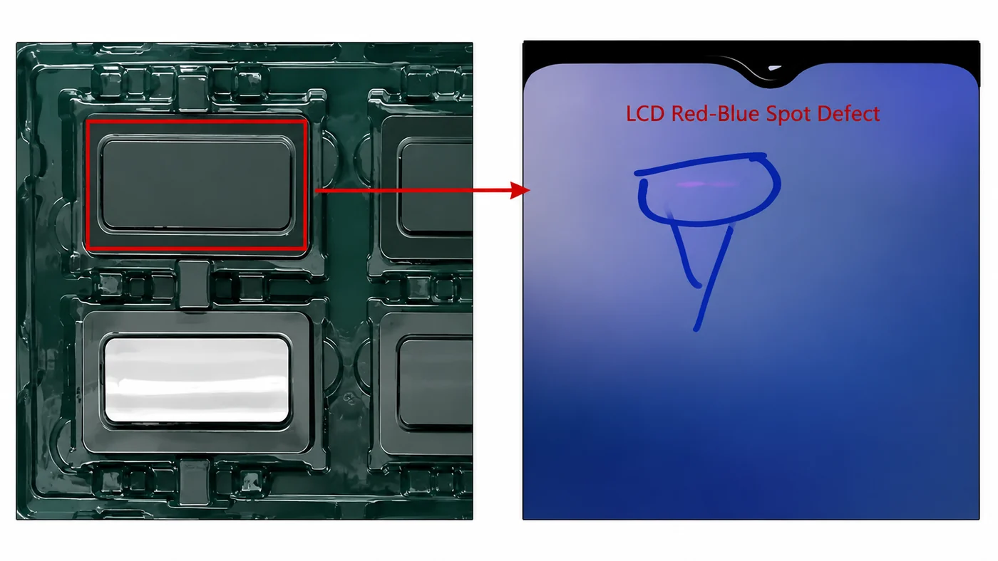
Small and medium TFT LCD modules are often packed in blister trays, placed in antistatic bags, and vacuumed. If the tray leaves too little Z-direction clearance, vacuum force can press the tray surface into the LCD module. The result can look exactly like a panel defect, even though the damage was introduced during packaging.
What To Include in an RFQ or Failure Analysis Request
When red/blue mura appears, the supplier needs more than one defect photo. The useful question is not only “Can you replace the LCD?” but “Where did the pressure enter the process, and how can it be controlled next time?”
For a new project, include the following details in the TFT LCD module RFQ or failure analysis request:
- Panel size, resolution, viewing mode, glass thickness, and final module stack.
- Photos under black screen, white screen, and power-off conditions.
- Whether the defect appears before or after lamination, bonding, packaging, or transport.
- Lamination pressure, vacuum level, bonding time, platform flatness, and cleaning method.
- Handling method, tray structure, vacuum packaging condition, and Z-direction tray clearance.
- Pressure-test method: force, rubber tip size, support fixture, pressure point, duration, and acceptance criteria.
This information helps the engineering team separate cell design weakness, module-process pressure, packaging stress, and customer-side handling damage. It also gives both sides a clearer basis for acceptance criteria. For broader project-level risk control, compare the defect review with the custom LCD project risk checklist and the LCD module sourcing risks checklist.
Where This Fits in the Engineering Library
This red/blue mura case belongs to the quality-control side of the TFT LCD module knowledge base. For the broader process flow, RFQ details, and supporting TFT-LCD structure topics, use the Engineering Resource Center as the main entry point.
For HMI projects where pressure, bonding, enclosure, and lifecycle risks must be reviewed together, see our industrial TFT LCD display modules.
Conclusion
TFT LCD red/blue mura is usually a pressure-related optical defect, not a simple electrical fault. The typical mechanism is glass deformation, photo-spacer movement, PI alignment layer scratch, and local light leakage from affected subpixels. The risk rises with larger panels, thinner glass, higher transmittance, and narrower black matrix margins.
The best prevention is practical: choose a panel structure with enough pressure margin, control thinning thickness, avoid active-area pressure in handling and splitting, tune bonding parameters, and design packaging with enough clearance. For engineering teams, the goal is not only to identify the defect but to remove the pressure path that created it.
Need a TFT LCD Defect Review?
SuccessLCD can help review TFT LCD module defects, pressure-sensitive designs, bonding risks, and packaging requirements before mass production. Start from the TFT LCD modules page or send the project details through the contact page.


