
Custom LCD Project Risk: Design to Production Checklist
A custom LCD project is safest when the display requirements, host electronics, mechanical stack, validation plan and component lifecycle are reviewed before tooling. This practical roadmap shows what to freeze at each stage so the project can move from concept to stable production with fewer redesign loops.
Quick answer: Control custom LCD project risk through five gates: requirement freeze, design review, engineering sample approval, reliability validation and production release. Each gate needs measurable acceptance criteria and an approved revision of the drawing, BOM, firmware and test plan.
Why Custom LCD Projects Fail
Most costly failures are not caused by the LCD panel alone. They come from incomplete system requirements: the interface is incompatible with the host processor, backlight heat cannot escape through the enclosure, the cover lens changes touch sensitivity, the FPC is stressed during assembly, or a critical component changes after qualification.
The engineering goal is therefore not to collect the longest specification. It is to identify decisions that affect fit, electrical compatibility, optical performance, reliability and supply continuity, then verify each decision before the next commitment.
If the project needs a modified outline, FPC, backlight, interface, touch panel, cover lens or optical bonding stack, use SuccessLCD’s custom TFT LCD engineering support to review feasibility before tooling.
Custom LCD Risk Control Matrix
| Risk area | Decision to freeze | Evidence before approval | Typical failure if missed |
|---|---|---|---|
| Application environment | Temperature, sunlight, humidity, vibration, ESD and operating duty | Written use profile and test conditions | Low contrast, condensation, resets or premature aging |
| Optical and thermal | Brightness, viewing angle, bonding method and heat path | Luminance, uniformity and thermal measurements in the final stack | Brightness decay, hot spots or poor sunlight readability |
| Interface and power | Host processor, interface, timing, voltages and power sequence | Compatible timing table, initialization code and bench test | White screen, flicker, EMI or unstable startup |
| Mechanical integration | Outline, active area, mounting, gasket, FPC route and connector | Controlled 2D drawing and enclosure stack review | Mura, light leakage, glass stress or assembly interference |
| Touch and cover lens | Glass, printing, bonding, gloves, water and noise environment | Touch tuning on the actual product assembly | False touches, dead zones or poor wet/glove operation |
| Lifecycle and quality | Approved BOM, change notice, traceability and inspection limits | Signed sample, BOM revision and production control plan | Uncontrolled substitutions or inconsistent production lots |
Five Gates from Design to Mass Production
- Requirement freeze: agree on the application, display performance, interface, mechanical envelope, environment, target quantity and lifecycle.
- Design review: confirm the optical stack, backlight and heat path, interface timing, FPC, connector, touch stack and enclosure tolerances.
- Engineering sample approval: test the sample in the real host system and enclosure; record every issue against a controlled revision.
- Reliability validation: run the agreed environmental, electrical and mechanical tests using acceptance limits defined before testing starts.
- Production release: approve the golden sample, BOM, drawings, firmware, inspection criteria, packaging and change-control process.
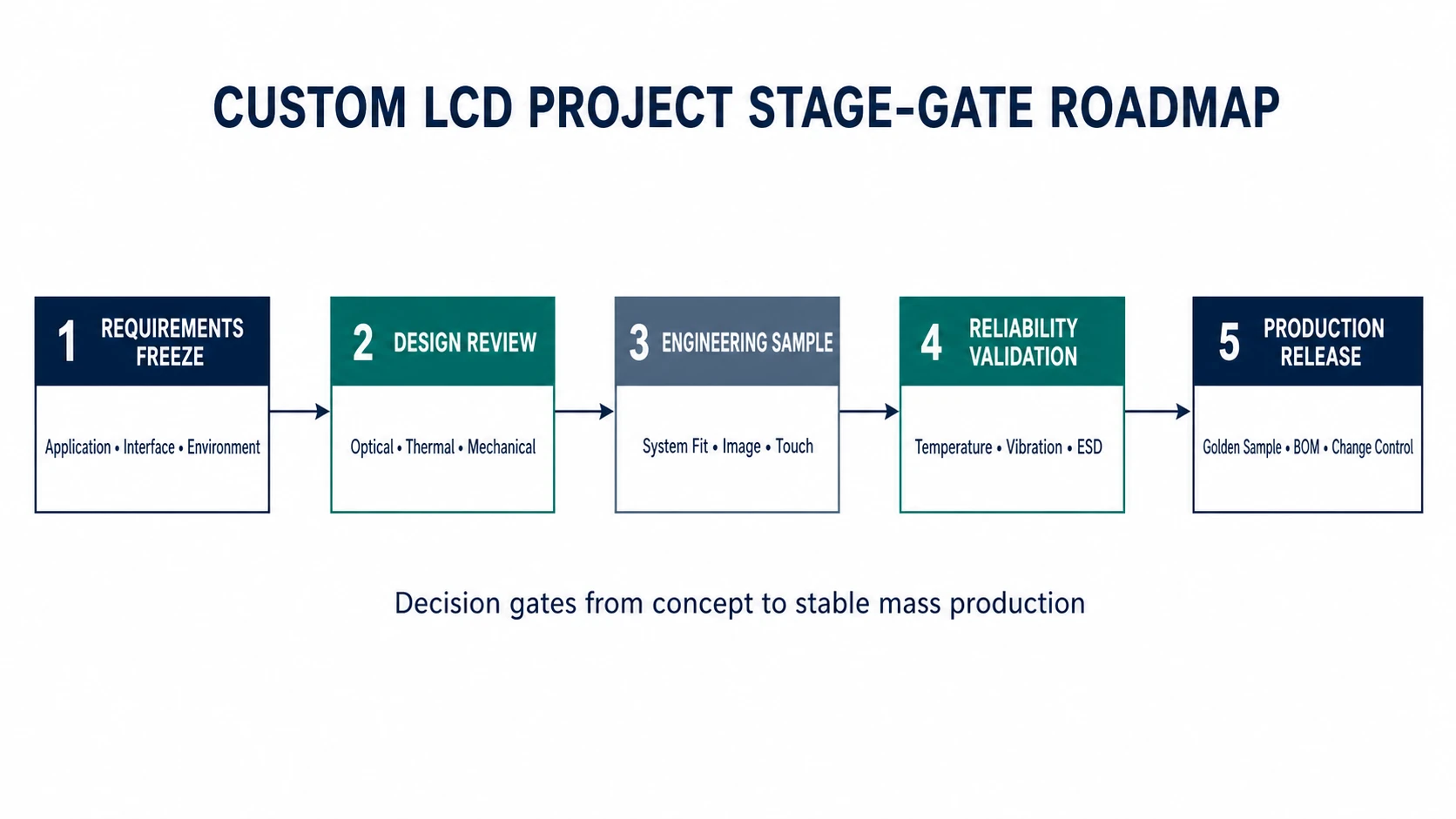
Gate rule: do not approve tooling, pilot production or mass production while an interface, mechanical or validation requirement is still described as “to be confirmed.” Assign an owner and closure date instead.
1. Requirements to Freeze Before Quotation
- Product application and expected service life
- Display size, resolution, active area and orientation
- Host processor and preferred display interface
- Brightness, viewing angle and optical bonding need
- Touch type, cover lens and operating conditions
- Operating and storage temperature ranges
- Mechanical outline, mounting and FPC direction
- Annual quantity, sample timing and launch date
- Required tests, certificates and inspection limits
- Lifecycle, change-notice and traceability expectations
Unknown items should be marked “open to engineering recommendation.” This tells the supplier where a design proposal is needed without creating a false fixed requirement. For a copy-ready input format, use the TFT LCD module RFQ checklist and template.
2. System Design Review Checklist
Interface, timing and power
- Confirm the host supports the selected RGB, LVDS, MIPI DSI, eDP, MCU or SPI interface without an avoidable bridge device.
- Review lane count, pixel clock, timing, voltage rails, reset behavior, initialization commands and power-up/power-down sequence.
- Check connector pinout, grounding, cable or FPC length and routing before the PCB layout is frozen.
The MIPI, LVDS and RGB LCD interface comparison explains the main compatibility and routing trade-offs.
Optical performance and heat
- Set brightness at the finished-product viewing surface, not only at the bare LCD.
- Evaluate cover lens, touch sensor, polarizer and bonding losses together with the ambient-light requirement.
- Confirm backlight current, power consumption and a practical heat path through the final enclosure.
- Measure luminance and uniformity after thermal stabilization, using agreed operating conditions.
Mechanical, touch and enclosure integration
- Control active area, view area, outline, bezel overlap, mounting points, gasket compression and connector clearance.
- Provide strain relief and a safe bend path for the FPC; avoid pulling the panel through the connector or housing.
- Test touch performance with the production cover lens, adhesive, enclosure ground, display noise and power supply.
- Define glove, water, palm-rejection and EMC conditions before touch firmware tuning.
For cover glass, printing, bonding and projected-capacitive touch decisions, review the touch panel and cover lens integration options.
3. Engineering Sample and Reliability Validation
Approve the engineering sample only after it has been tested in the actual host electronics and representative enclosure. A bench image is useful, but it does not prove thermal, touch, EMI or mechanical performance in the final product.
| Validation group | What to check | Release evidence |
|---|---|---|
| Visual and optical | Brightness, uniformity, color, viewing angle, mura, dead pixels and contamination | Measured report plus approved cosmetic standard |
| Electrical | Startup, reset, image stability, timing margin, current, touch communication and ESD recovery | System test log using the target host |
| Mechanical | Fit, clearances, connector access, FPC stress, gasket load and assembly sequence | Signed drawing and assembly review |
| Environment | Temperature, humidity, vibration, sunlight or other application-specific stresses | Agreed test conditions, sample count and pass limits |
When a sample fails, record the symptom, test condition, affected revision, root cause, corrective action and retest result. Avoid informal changes that are not reflected in the drawing, BOM or firmware version.
4. Production Release and Lifecycle Control
Mass-production approval should lock the configuration that passed validation. The release package should include:
- Approved golden sample and sample revision
- Final LCD, FPC, backlight, touch and cover-lens drawings
- Approved BOM and critical-component list
- Firmware, initialization code and touch parameters
- Incoming and outgoing inspection criteria
- Reliability report and unresolved deviation list
- Packaging, labeling and lot-traceability rules
- Product-change notice and end-of-life process
Supplier quality terms should define how component substitutions, process changes and end-of-life notices are reviewed. The LCD module sourcing risk checklist covers the commercial and lifecycle controls that complement this engineering roadmap.
Custom LCD Project Risk FAQs
What is the most expensive custom LCD project mistake?
Freezing tooling or the host PCB before the interface and mechanical stack are verified is usually the most expensive mistake. It can force changes to the FPC, connector, enclosure, backlight or main board after parts have already been ordered.
When should a project use a standard module instead?
Use a standard module when the size, resolution, interface, brightness, temperature range and mechanical outline already fit the product. Choose customization only when a real system requirement justifies changes such as FPC, backlight, touch, cover lens, bonding or outline.
What must be approved before mass production?
Approve the golden sample, final drawings, BOM revision, firmware, touch parameters, inspection criteria, reliability results, packaging and change-control process. Every production lot should be traceable to this released configuration.
Copyable gate-review record: Project and drawing revision: ____; requirement or risk: ____; supporting evidence: ____; open question: ____; responsible team: ____; next decision date: ____; approval status: ____. Use one record for each unresolved item before tooling or production release.
Review Your Custom LCD Project Before Tooling
Send the application, host processor, display size, interface, brightness, touch, mechanical drawing, environment, schedule and annual quantity. The engineering team can identify compatibility and production risks before you commit to samples or tooling.
Send Project Requirements


