
TFT-LCD Array Process: 5-Mask Flow & Fabrication Steps
Updated · Technical Guide Reviewed.
The TFT-LCD array process fabricates the pixel-switching backplane on glass. In the representative five-mask flow below, the patterned levels are gate metal, semiconductor island, source/drain metal, passivation with contact vias, and pixel ITO. Deposition, photolithography, etching and stripping are repeated as the structure is built.
Use this guide to follow the fabrication sequence and its control points. For the completed layer stack and pixel circuit, use the Array Substrate Structure Guide. The five-mask sequence is a representative a-Si TN example; confirm the actual panel architecture and process with its manufacturer.
What Does The TFT-LCD Array Process Include?
TFT-LCD panel manufacturing is normally divided into Array fabrication, color-filter fabrication, and cell assembly. The Array stage creates the switching backplane. The color-filter stage forms the RGB and black-matrix structures. Cell assembly aligns and bonds the two glass substrates and fills the cell with liquid crystal.
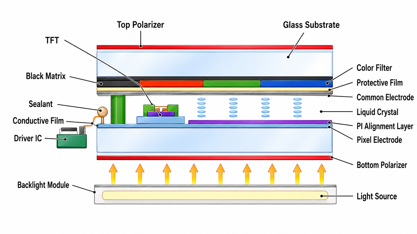
Driver IC bonding, polarizer attachment, backlight integration, touch-panel bonding, housing, and final module testing occur later. Keeping these stages separate helps engineers distinguish a panel-level Array issue from a downstream module-integration issue.
5-Mask TFT-LCD Array Process Flow
A common 5-mask a-Si TN flow uses five lithography cycles. The exact sequence can vary, but the functional pattern is consistent:
| Mask | Main Pattern | Function | Typical Process |
|---|---|---|---|
| 1 | Gate electrode and scan line | Selects the pixel row | Metal deposition, lithography, wet etching |
| 2 | Gate insulator, a-Si, and N+ a-Si island | Forms the insulated semiconductor channel stack | PECVD, lithography, dry etching |
| 3 | Source/Drain electrodes and data line | Connects the signal line to the TFT channel | Metal deposition, lithography, metal and N+ etching |
| 4 | Passivation and contact via | Protects the TFT and opens the pixel-electrode connection | PECVD, lithography, dry etching |
| 5 | Pixel ITO electrode | Creates the transparent electrode that drives the liquid crystal | ITO deposition, lithography, ITO etching |
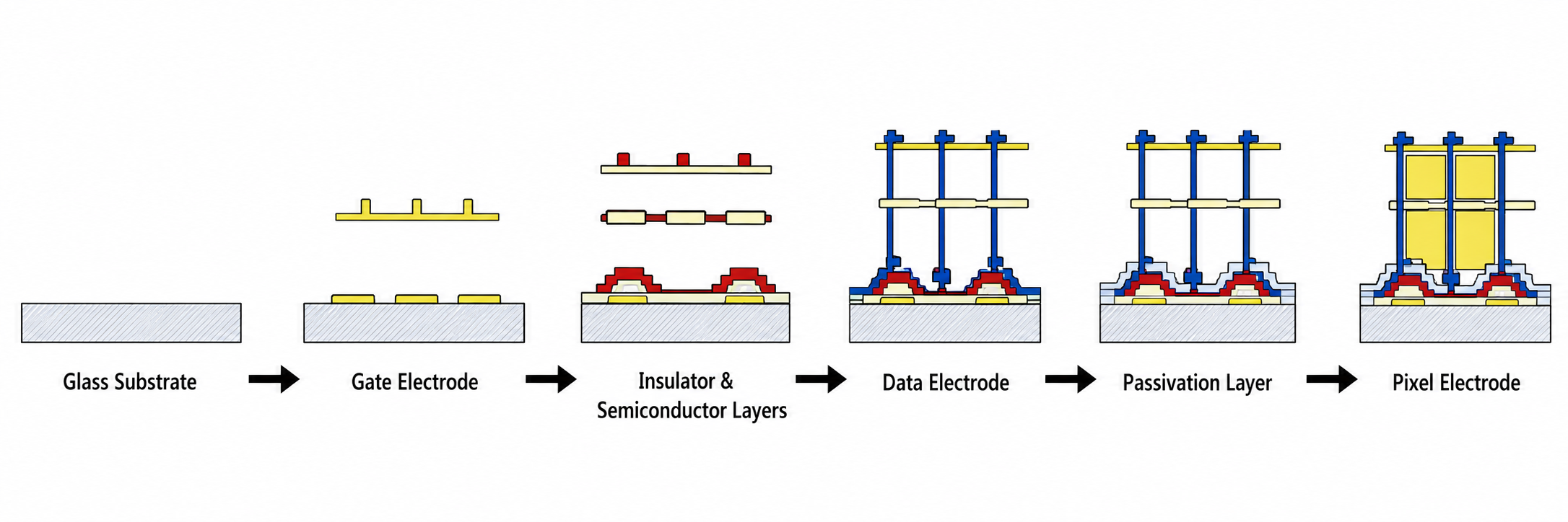
The mask count is a process-design choice, not a universal quality grade. Viewing mode, aperture-ratio target, reliability requirements, and factory integration strategy can change the number of patterned layers. See the 5-mask TFT process guide for the detailed mask-by-mask sequence.
5-Mask Vs 6-Mask Array Flows
A 5-mask flow is a useful reference for a conventional a-Si TN backplane. An IPS or FFS design may use a sixth mask to pattern a common electrode or another optical/electrical layer. Factory-specific integration can combine or separate patterning steps, so two panels with the same viewing mode do not necessarily use identical mask sequences.
| Comparison | 5-Mask Reference | 6-Mask Reference |
|---|---|---|
| Typical use | Conventional a-Si TN architecture | IPS/FFS or another structure with an additional patterned electrode |
| Process impact | Fewer lithography cycles and overlay steps | One additional deposition/patterning cycle and its process controls |
| Selection rule | Judge the complete panel architecture, optical target, reliability, and factory capability—not mask count alone. | |
TFT-LCD Array Substrate Structure
A TFT Array contains a matrix of pixel switches. The gate line selects a row, the data line supplies the pixel signal, and the TFT charges the pixel electrode. A storage capacitor helps hold the voltage between refresh cycles.
In a common bottom-gate a-Si structure, the layer stack includes the glass substrate, gate metal, gate insulator, a-Si semiconductor, N+ a-Si ohmic contact, Source/Drain metal, passivation, contact via, and pixel ITO. IPS and FFS structures add patterned common-electrode features according to the panel design.
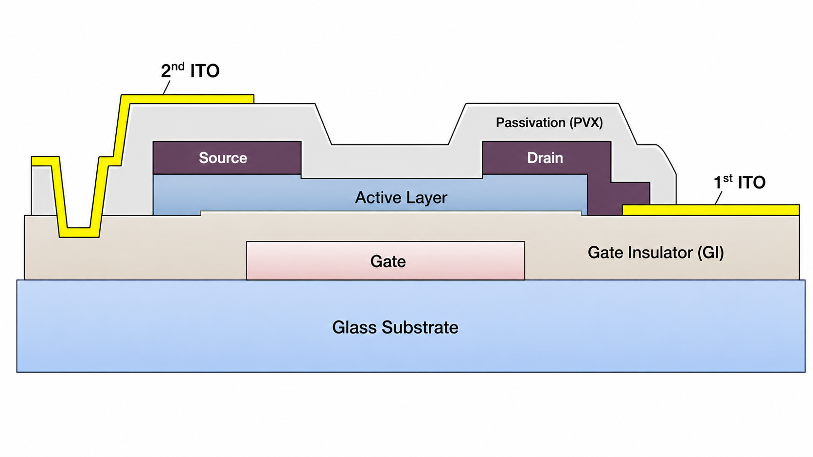
For a detailed layer-by-layer explanation, see the TFT-LCD Array substrate structure guide.
The Repeated Photolithography Cycle
Each mask level uses the same core pattern-transfer logic:
- Film deposition: PVD commonly forms conductive metal or ITO films; PECVD commonly forms SiNx and a-Si films.
- Photoresist coating: a uniform resist layer is applied to the glass.
- Exposure: the photomask transfers the required pattern into the resist.
- Development: the soluble resist region is removed.
- Etching: exposed film is removed by wet or dry etching.
- Stripping: the remaining photoresist is removed before the next layer is deposited.
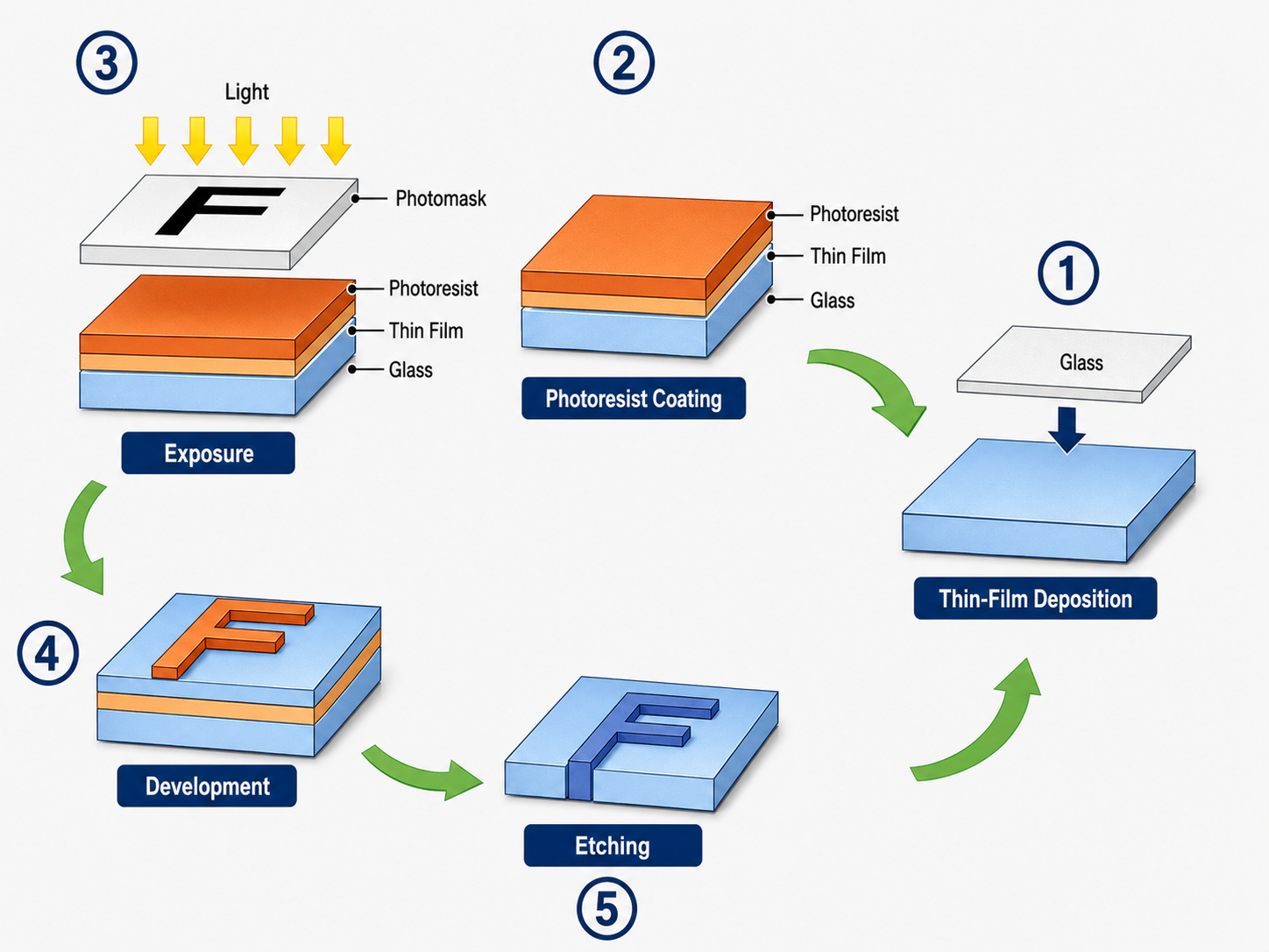
Metal layers are often patterned by wet etching, while semiconductor and insulating films commonly use plasma-based dry etching. The process window must control line width, overlay, film residue, sidewall profile, and contact integrity. Read the TFT-LCD photolithography guide for a deeper process explanation.
TFT-LCD Array Materials And Their Functions
| Material | Primary Role | Engineering Concern |
|---|---|---|
| Alkali-free glass | Dimensionally stable substrate for the complete backplane | Thermal shrinkage, chemical resistance, low mobile-ion contamination |
| Al or Cu metal stacks | Gate, scan, Source/Drain, and data-line conductors | Resistance, adhesion, hillocks, corrosion, and diffusion control |
| a-Si and N+ a-Si | Semiconductor channel and low-resistance ohmic contact | Mobility, contact resistance, uniformity, and device stability |
| SiNx | Gate insulator and protective passivation | Interface quality, pinholes, moisture barrier, and etch compatibility |
| ITO | Transparent pixel or common electrode | Sheet resistance, optical transmission, etch profile, and durability |
For more detail, use the TFT-LCD Array materials guide and the focused comparison of copper vs aluminum Gate electrodes.
How Array Design Affects Panel Performance
Array process decisions influence the finished panel even though the backplane is only one manufacturing stage:
- Line resistance and RC delay: Gate and data-line resistance affect signal timing, especially as panel size and resolution increase.
- Aperture ratio: narrower routing and compact TFT geometry can leave more transparent area for the pixel, improving optical efficiency.
- Uniformity: film thickness, critical dimensions, contact resistance, and TFT characteristics must remain uniform across the glass to reduce visible mura.
- Retention and stability: leakage current, charge trapping, contamination, and unstable interfaces can contribute to image-retention or switching problems.
These relationships are useful during failure analysis, but a visible symptom should not be assigned to the Array stage without measurement. Backlight, driver, timing, optical-film, cell-gap, bonding, and application conditions can produce similar symptoms. For examples, see the TFT-LCD image-retention guide and the red/blue mura case study.
Common Array Process Defects
| Defect | Possible Array-Level Cause | Typical Effect |
|---|---|---|
| Open line | Metal discontinuity, particle, incomplete deposition, or over-etch | Missing row, column, or local pixel group |
| Short circuit | Residue, under-etch, particle bridge, or overlay error | Abnormal row/column drive or clustered pixel defects |
| High contact resistance | Via residue, poor interface, or insufficient contact opening | Weak charging, delay, or unstable pixel voltage |
| TFT leakage or threshold shift | Semiconductor damage, contamination, interface traps, or passivation failure | Voltage loss, nonuniformity, retention, or unstable grayscale |
Factory electrical testing and automated optical inspection identify many of these defects before cell or module assembly. Root-cause confirmation may require line measurements, pixel electrical data, cross-section analysis, and process-history review.
What Engineers And Display Buyers Should Verify
Most OEM buyers do not specify every Array mask. The process knowledge is useful for understanding panel limits, comparing architectures, and diagnosing risk. Before qualifying a TFT-LCD panel or module, confirm:
- the TFT technology and viewing mode: a-Si, oxide, or LTPS; TN, IPS, or FFS;
- the operating temperature, brightness, lifetime, image-retention, and reliability targets;
- whether the selected panel is a stable production item with suitable lifecycle support;
- the downstream module requirements: interface, backlight, touch stack, optical bonding, FPC, and mechanical outline;
- the validation plan for samples, environmental testing, and change control.
Frequently Asked Questions
What Is The TFT-LCD Array Process?
It is the front-end manufacturing process that creates the active-matrix TFT backplane on glass through repeated film deposition, photolithography, etching, and stripping.
What Is A 5-Mask TFT Process?
It is an a-Si TFT-LCD Array flow that typically patterns the Gate layer, semiconductor island, Source/Drain layer, passivation/via layer, and pixel ITO electrode in five lithography cycles.
Is A Higher Mask Count Always Better?
No. Mask count depends on panel architecture and factory process integration. More masks can support additional structures but also add process steps, alignment requirements, and cost.
Why Is Alkali-Free Glass Used?
Mobile alkali ions can affect TFT characteristics and liquid-crystal reliability. Alkali-free glass also provides the thermal and dimensional stability needed for large-area thin-film processing.
Technical References
- Applied Materials: Amorphous Silicon for display backplanes
- AGC: Alkali-Free Glass Substrates For TFT Displays — substrate stability and alkali contamination.
- Applied Materials: AKT-PECVD For Amorphous Silicon — PECVD of semiconductor and insulating films for the TFT backplane.
Related Deep-Dive Guides
- TFT-LCD Array substrate structure
- 5-mask TFT-LCD Array process
- TFT-LCD Array photolithography
- TFT-LCD Array materials
- Copper vs aluminum Gate electrodes
From Array Requirements To Module Selection
For a finished display project, compare TFT LCD Module Options and their actual size, resolution and interface. The 7-Inch 1024×600 RGB Reference shows the type of module information to review. Use the Custom TFT Engineering Process when the host, FPC, optical stack or enclosure needs adaptation.
Bring the host interface, mechanical space, brightness and touch needs, environment, quantity and lifecycle requirements. Module customization and sample validation are separate from choosing an Array mask count.
Discuss an LCD Project


