
TFT LCD Module Manufacturing Process Guide
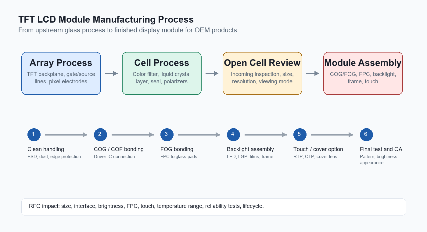
TFT LCD module manufacturing is the assembly process that turns a finished LCD cell into a product-ready display. It adds the driver IC, FPC or connector, polarizers, backlight, frame, optional touch panel or cover lens, and final inspection after the upstream Array and Cell stages.
For OEM teams, this stage determines interface compatibility, FPC direction, backlight performance, mechanical fit, touch integration and final test requirements. For the optical components, see our LCD backlight module guide. For outdoor viewing, continue with the TFT LCD sunlight readability guide.
Key takeaways
- The complete TFT LCD production chain is usually divided into Array, Cell, and Module stages.
- Module assembly adds COG or COF driver ICs, FPC bonding, polarizers, backlight, frame, optional touch panel, and final test.
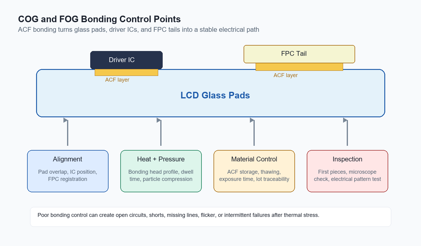
- COG bonding and FOG bonding rely on ACF, alignment accuracy, pressure, temperature, time, and particle compression control.
- Backlight design affects luminance, uniformity, power, temperature rise, lifetime, and outdoor readability.
- A good RFQ should define size, resolution, interface, brightness, touch, mechanical stack, operating environment, and reliability needs before sampling.
In this guide
- What TFT LCD module manufacturing means
- The full process flow
- COG, FOG, COF, and COB bonding choices
- Backlight and optical assembly
- Testing and reliability checks
- RFQ checklist
What Is TFT LCD Module Manufacturing?
It is the final assembly stage after Array and Cell fabrication. Manufacturers bond the driver IC and FPC, add the backlight and frame, integrate optional touch or cover glass, and test the finished module against electrical, optical and mechanical requirements.
For module selection, start with custom TFT LCD modules. For the upstream backplane, the TFT-LCD Array process guide explains how the transistor matrix is built before module assembly.
For a concrete module comparison, review the 7-Inch RGB Module Reference and 5-Inch LVDS Module Reference. Check the host output, full pin assignment, timing and FPC routing against the chosen reference. Final configuration and suitability require confirmation for your project.
TFT LCD Manufacturing Process: Array, Cell, and Module
The complete TFT LCD production path is commonly understood in three large stages:
- Array process: builds the TFT backplane, gate/source lines, pixel electrodes, insulating layers, and related thin-film structures on glass.
- Cell process: combines the TFT array substrate with the color filter substrate, alignment layers, spacer control, seal pattern, liquid crystal filling or one-drop filling, and polarizer preparation.
- Module process: adds driver ICs, FPC, backlight, frame, touch panel, cover lens, inspection, aging, packing, and project-specific customization.
This article focuses on the module process because it is closest to OEM display sourcing. Array and Cell process choices still matter, especially for aperture ratio, material stack, electrical behavior, and display defects. For material background, review the TFT-LCD Array materials guide.
For the manufacturing boundary, AUO's 2023 Annual Report (Page 80) separates Array, Cell and Module assembly. Hung Chun Chang's 2018 TFT-LCD Module And Package Process Chapter describes downstream polarizer attachment, driver bonding, module assembly and packing. The six steps below are an OEM review framework; confirm the exact process and acceptance criteria for the chosen module.
Step 1: Engineering Review and Incoming LCD Cell Control
Engineering first confirms the cell size, active area, resolution, viewing mode, interface, temperature range and backlight target. Incoming inspection then checks glass edges, polarizer condition, visible defects, lot traceability and electrical compatibility.
This prevents a common sourcing error: choosing a panel by size and resolution alone. A mechanically similar cell can still fail if the FPC direction, connector, interface, brightness or temperature range does not fit the product.
Step 2: Clean Handling, Polarizer, and Surface Preparation
LCD cells are sensitive to dust, fingerprints, electrostatic discharge and edge stress. Clean trays, ESD controls and careful handling reduce particles, scratches, pressure marks and bonding defects before assembly.
Polarizers may arrive attached or be added during module preparation. Alignment, bubbles, scratches and contamination must be checked before volume production because defects become harder to correct after bonding and frame assembly.
Step 3: Driver and FPC Bonding: COG, COF, FOG, and COB
The driver circuit must connect the host signal to the TFT array. Several bonding terms appear in LCD module manufacturing, and they are easy to mix up.
| Bonding method | Meaning | Typical use | Main control point |
|---|---|---|---|
| COG | Chip on Glass | Driver IC bonded directly on LCD glass | IC alignment, ACF compression, temperature, pressure, time |
| COF | Chip on Film | Driver IC mounted on flexible film | Film handling, pitch, bend reliability, connection stability |
| FOG | Film on Glass | FPC or flexible film bonded to glass pads | Pad alignment, hot-bar profile, ACF particle contact |
| COB | Chip on Board | More common in simpler LCD modules where IC is mounted on PCB | PCB assembly, wire bonding or encapsulation, board-level protection |
Modern small and medium TFT LCD modules often use COG plus FPC bonding. Larger or high-resolution designs may use COF, depending on panel architecture and driver layout. COB is still important in the broader LCM world, especially for monochrome or simpler modules, but it is not the default structure for many current TFT open-cell assemblies.
Why ACF Control Matters
COG and FOG processes commonly rely on ACF, or anisotropic conductive film. ACF conducts through the thickness direction after heat and pressure compress conductive particles between matching pads, while maintaining insulation between neighboring pads.
The engineering lesson is more important than any single number: ACF must be stored, thawed, handled, aligned, compressed, and inspected as a controlled material. Poor ACF control can cause open circuits, shorts, intermittent display failure, line defects, or failures after thermal cycling.
Step 4: Backlight Assembly and Optical Stack
A TFT LCD cell controls light but does not create light. The backlight unit provides the illumination that passes through the optical films, lower polarizer, liquid crystal layer, color filter, and upper polarizer. A typical edge-lit module may include LEDs, light guide plate, reflector, diffuser, prism films, tape, frame, and connection to the FPC or backlight cable.
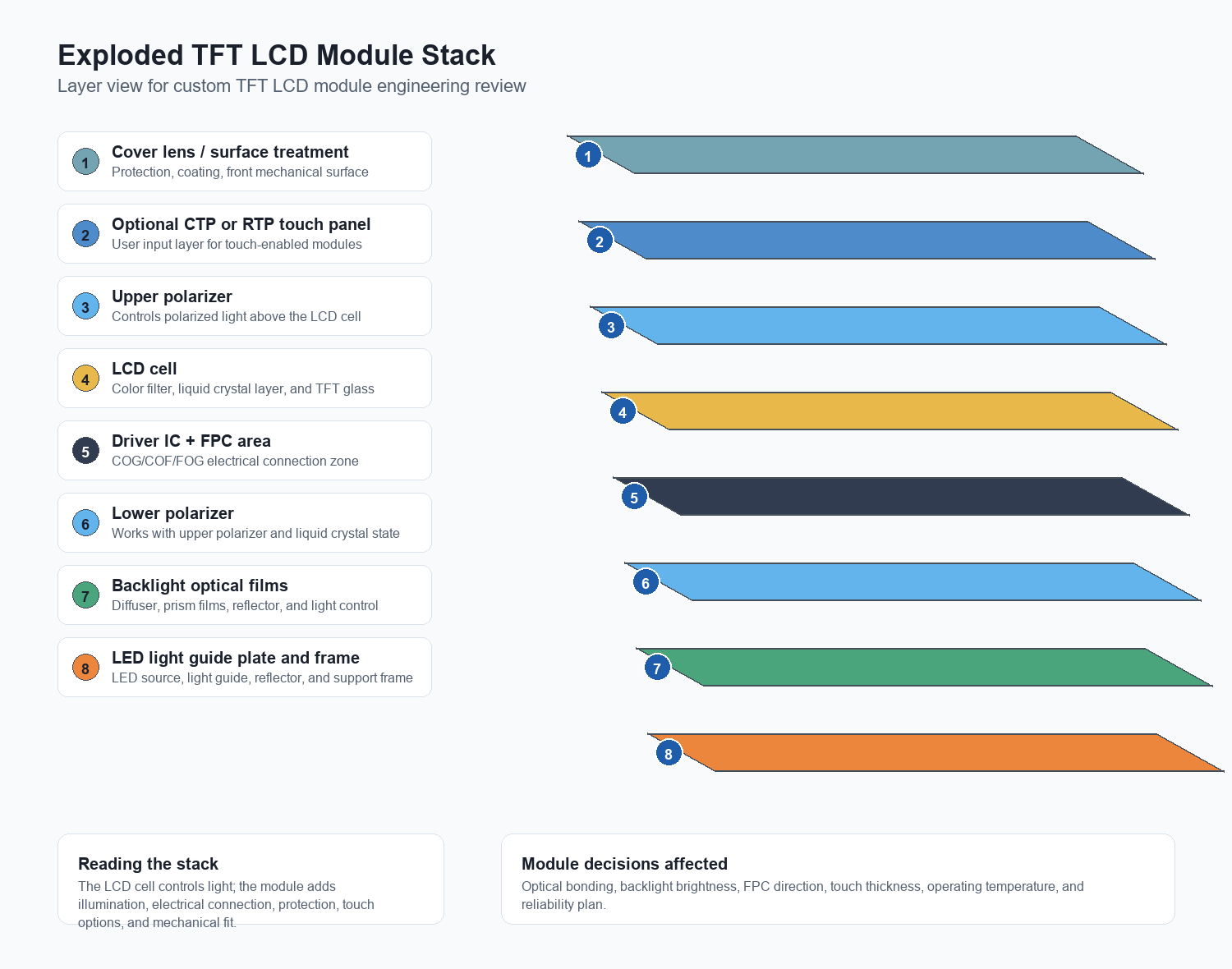
Backlight design affects several practical specifications:
- Luminance: indoor modules may use around 250 to 500 cd/m2, while outdoor-facing or high-brightness designs may target 700 to 1000 cd/m2 or more.
- Uniformity: LEDs, light guide pattern, diffuser, prism films, and frame pressure all influence visible hot spots or dark areas.
- Power: higher brightness increases LED current, thermal load, and battery or power-supply demand.
- Lifetime: LED current, heat, optical film aging, and operating temperature affect long-term luminance decay.
- Mechanical thickness: slim modules need tighter control of light guide thickness, film stack, tape, and frame clearance.
For sunlight-readable or sealed industrial products, review brightness together with cover glass, optical bonding, anti-glare treatment and heat dissipation. A brighter backlight alone does not solve reflection or enclosure heat. Automotive projects should also consider PGU heat and optical loss; see the automotive HUD TFT LCD display guide.
Step 5: FPC, Connector, Touch Panel, and Mechanical Integration
The FPC is more than a cable. It carries display signals, power, ground, backlight lines, touch signals, and sometimes component pads. Its direction, length, stiffener position, connector pitch, bend radius, and pin assignment must match the customer PCB and enclosure.
Touch integration adds another layer of decisions. A resistive touch panel may fit pressure or stylus input, while projected capacitive touch is common for multi-touch and sealed front designs. Cover lens thickness, optical bonding, AG/AR/AF coatings and controller tuning should be reviewed together; see our touch panel and cover lens options.
If the interface has not been selected yet, use the TFT LCD interface guide before finalizing the FPC and connector. Interface choice can change pin count, EMI behavior, PCB routing, software workload, and cable length constraints.
Step 6: Electrical Test, Appearance Inspection, and Reliability Review
Testing is not a single final gate. A practical module line may include first-piece inspection, bonding inspection, semi-finished electrical test, backlight check, touch test, full functional test, appearance inspection, QA sampling, and packing inspection.
Typical checks include:
- Display on/off and image pattern test
- Missing line, abnormal display, flicker, black dot, white dot, and mura check
- Backlight brightness, color, current, and uniformity check
- Touch function and coordinate response if touch is integrated
- FPC alignment, solder or hot-bar bonding area, insulation tape, and connector condition
- Outer appearance: glass edge, polarizer surface, frame, tape, cover lens, and label
For reliability, the test plan should match the final application. Industrial HMIs, vehicle-adjacent equipment, outdoor devices, medical instruments, and handheld terminals do not face the same risk profile. Common requirements may include high temperature operation, low temperature operation, high temperature storage, low temperature storage, damp heat, thermal cycling, vibration, ESD, drop, connector durability, and backlight aging.
Critical Control Points in LCD Module Assembly
| Process point | Why it matters | Common risk if poorly controlled | What to confirm in production |
|---|---|---|---|
| Cell handling | Protects glass, polarizer, and optical surface | Scratch, particle, edge crack, pressure mark | Clean handling, ESD control, tray control |
| COG bonding | Connects driver IC to glass pads | Open, short, line defect, intermittent failure | Alignment, ACF condition, bonding profile, first-piece inspection |
| FOG bonding | Connects FPC or film to glass | Weak connection, shifted FPC, poor bend reliability | Pad overlap, pull strength, hot-bar parameters, visual check |
| Backlight assembly | Controls luminance and uniformity | Dark spot, light leakage, high current, thermal stress | LED bin, film order, dust control, current and brightness test |
| Touch and cover lens | Defines front user interface | Newton rings, bubbles, touch drift, reflection | Bonding method, cover thickness, coating, touch controller |
| Final test | Confirms module is usable before shipment | Escaped display defect or assembly defect | Pattern test, appearance standard, QA sampling, packing check |
How Manufacturing Choices Affect Your RFQ
A useful RFQ covers more than screen size. It gives the supplier enough information to evaluate cell selection, bonding route, backlight, FPC, touch stack, mechanical fit and test requirements.
For a first RFQ, include the following:
- Diagonal size, active area, resolution, and viewing direction
- Interface: SPI, MCU, RGB, LVDS, MIPI DSI, eDP, or open to recommendation
- Host processor model, operating system, refresh-rate target, and color depth
- Brightness target, backlight voltage/current, and dimming method
- Operating and storage temperature range
- Touch requirement: no touch, RTP, or CTP
- Cover lens, optical bonding, anti-glare, anti-reflective, or anti-fingerprint needs
- FPC direction, connector type, connector pitch, pin count, and cable length
- Mechanical outline, thickness limit, mounting method, and enclosure window
- Reliability tests, inspection level, annual quantity, and expected lifecycle
For a more complete purchasing format, use the TFT LCD module RFQ checklist. For industrial equipment, the industrial HMI TFT LCD selection guide can help connect module manufacturing choices with field conditions.
Practical Checklist Before Sampling
Before ordering samples, use this short engineering checklist:
- Has the display size been checked against enclosure, PCB, and viewing distance?
- Can the host processor support the selected interface without an extra bridge IC?
- Is the FPC direction compatible with the board connector and assembly path?
- Is the backlight brightness high enough without creating unacceptable heat?
- Does the touch or cover lens stack change optical bonding, thickness, or reflection?
- Are the operating temperature and storage temperature realistic for the end device?
- Are reliability tests defined before tooling or mass production?
- Does the inspection standard cover display defects, backlight defects, FPC defects, and appearance defects?
Frequently Asked Questions
What is the difference between TFT LCD manufacturing and TFT LCD module manufacturing?
TFT LCD manufacturing can refer to the full Array, Cell, and Module chain. TFT LCD module manufacturing specifically focuses on turning the LCD cell into a finished module by adding driver ICs, FPC, backlight, frame, optional touch, testing, and packing.
What is COG bonding in a TFT LCD module?
COG means Chip on Glass. In a TFT LCD module, the driver IC is bonded directly to glass pads, commonly through ACF. The process requires accurate alignment, controlled heat, pressure, time, and inspection because weak bonding can cause open circuits, line defects, or intermittent failures.
What is FOG bonding?
FOG means Film on Glass. It usually refers to bonding an FPC or flexible film to the LCD glass connection area. FOG quality depends on pad overlap, hot-bar parameters, ACF condition, FPC handling, and mechanical bend reliability after the module is installed.
Why is the backlight important in TFT LCD module assembly?
The backlight determines brightness, uniformity, power consumption, heat, thickness, and long-term luminance stability. A high-brightness module may need stronger LED design, better thermal review, optical bonding, and surface treatment instead of simply increasing LED current.
What information should I send before requesting a custom TFT LCD module?
Send the display size, resolution, interface, host processor, brightness target, backlight electrical limits, touch or cover lens need, FPC direction, connector requirements, operating environment, reliability tests, annual quantity, and lifecycle expectation. These details help the supplier choose a feasible module path.
Conclusion
The TFT LCD module manufacturing process turns the cell into a product-ready component through driver and FPC bonding, backlight integration, mechanical assembly and final testing. These choices affect fit, performance and reliability beyond the basic panel datasheet.
If your project is moving from display selection to sampling, define the module-level requirements early. Review custom TFT LCD modules, confirm the interface with the TFT LCD interface guide, and prepare a clear TFT LCD module RFQ checklist before locking the PCB or enclosure.
For a supplier review, ask which manufacturing and inspection steps apply to the proposed module, which organization performs them, and what controlled drawing, inspection criteria and change record will be supplied. Review SuccessLCD manufacturing and inspection information alongside the module-specific proposal.
Prepare Your TFT LCD Module RFQ
Before sample production, align the LCD cell, interface, FPC direction, backlight target, touch structure, mechanical outline and reliability requirements. A clear RFQ reduces redesign and helps the factory choose a practical module assembly route.


