
TFT LCD Photolithography Process and Etching Steps
TFT-LCD array manufacturing guide
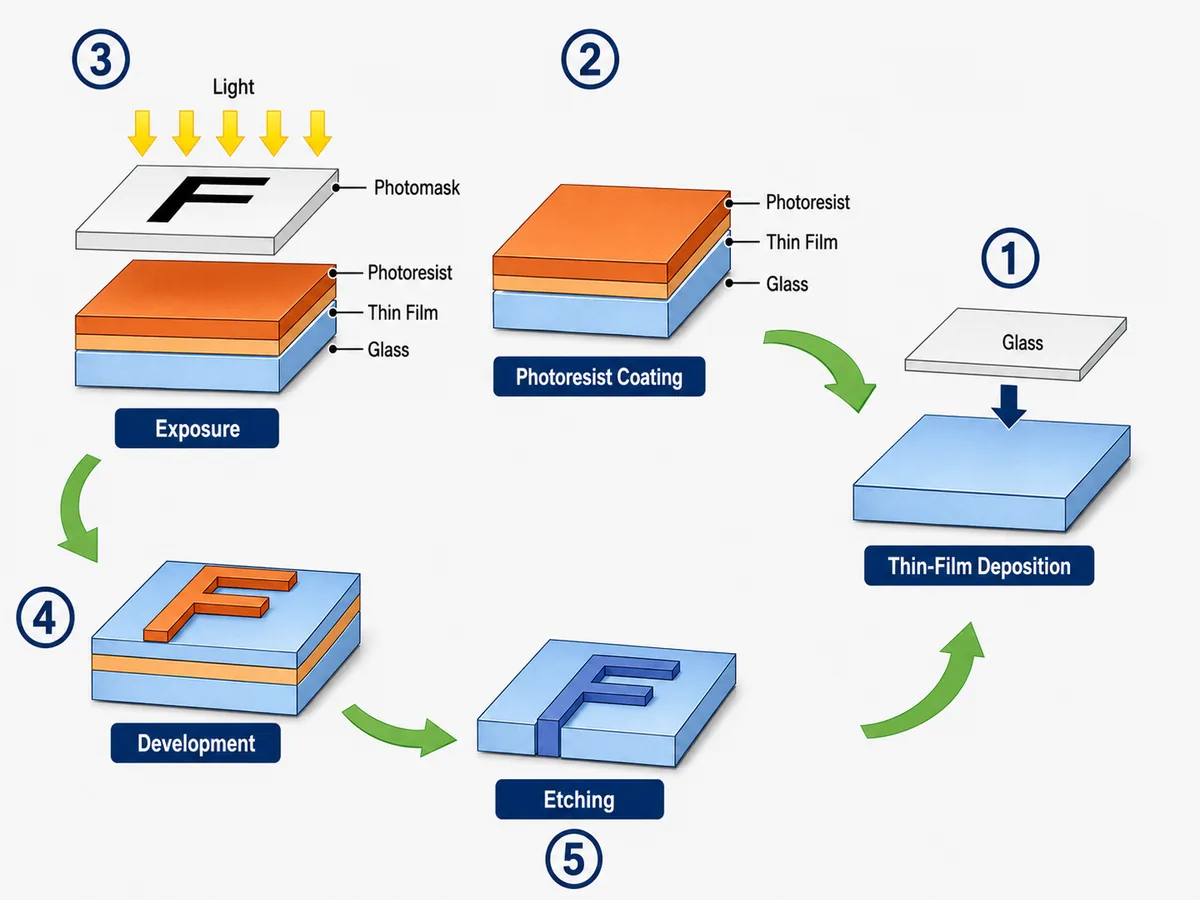
TFT LCD photolithography transfers a photomask pattern into each deposited film on the glass substrate. The core cycle is film deposition, photoresist coating, exposure, development, etching and resist stripping.
On this page
- The five main photolithography steps
- 1. Deposit the functional film
- 2. Coat and prepare the photoresist
- 3. Expose and develop the mask pattern
- 4. Choose wet or dry etching for the layer
- 5. Strip the photoresist and inspect the result
- How photolithography fits the TFT-LCD array flow
- TFT LCD photolithography FAQ
- Technical references and related guides
The five main photolithography steps
| Step | Purpose | Key control point |
|---|---|---|
| 1. Film deposition | Place the metal, semiconductor, dielectric or transparent conductor on the glass. | Thickness, uniformity, adhesion and particle control |
| 2. Photoresist coating | Create a photosensitive layer that can carry the mask pattern. | Coating thickness, edge condition and bake control |
| 3. Exposure and development | Transfer the photomask image into the photoresist. | Overlay alignment, dose, focus and developed dimensions |
| 4. Wet or dry etching | Remove film not protected by the patterned resist. | Selectivity, profile, undercut, residue and over-etch |
| 5. Resist stripping | Remove remaining photoresist before inspection and the next layer. | Residue removal without damaging the patterned film |
1. Deposit the functional film
The cycle begins with a controlled thin film on the glass substrate. Physical vapour deposition such as sputtering is commonly used for conductive films. Chemical vapour deposition or plasma-enhanced CVD can be used for semiconductor and dielectric films. The actual method depends on the layer material and process design.
Before patterning starts, thickness, uniformity, adhesion and contamination must be within the process window. A photolithography step cannot correct a defective deposited film.
2. Coat and prepare the photoresist
Photoresist provides the temporary protective pattern used during etching. Positive resist becomes more soluble in the exposed areas, while negative resist cross-links in the exposed areas and leaves the opposite pattern after development.
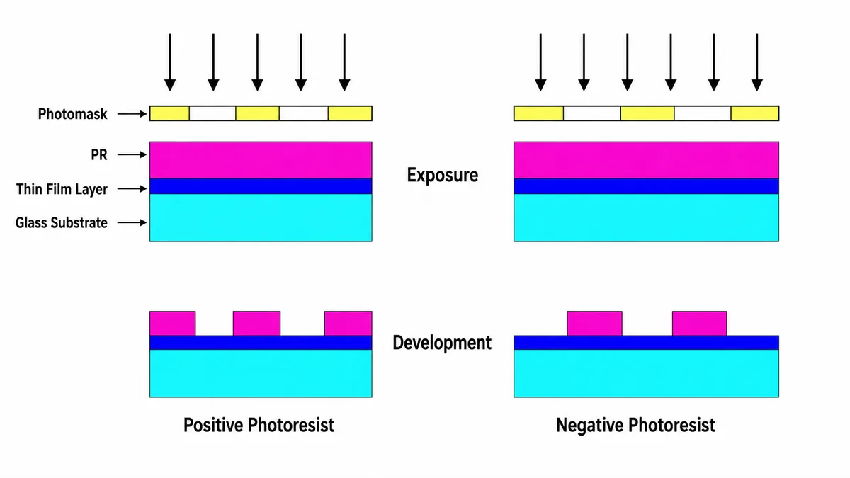
Positive resist is widely used in display-array processing, but the selected resist and bake conditions depend on the tool set, film stack, resolution and etch requirement. Coating thickness, soft bake and edge condition affect later exposure and development results.
3. Expose and develop the mask pattern
During exposure, ultraviolet light transfers the photomask pattern into the resist. Development then removes the soluble resist region and reveals the film to be etched.
Overlay alignment is critical because each new layer must connect with structures created by previous masks. Exposure dose, focus, resist thickness and development time influence the final line width and opening size. Inspection should confirm pattern completeness before etching.
4. Choose wet or dry etching for the layer
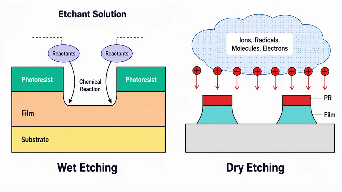
Wet etching removes material through a liquid chemical reaction. Dry etching uses plasma-generated reactive species in a controlled chamber. The choice is not based only on whether a layer is “metal” or “nonmetal.” It also depends on material chemistry, selectivity, profile, feature size, uniformity and acceptable substrate damage.
| Etch method | Typical advantage | Typical review point |
|---|---|---|
| Wet etching | High throughput and useful material selectivity for suitable films | Isotropic undercut, bath control, residue and uniformity |
| Dry etching | Better profile control for many fine-pattern or multilayer requirements | Plasma damage, selectivity, sidewall profile and chamber condition |
5. Strip the photoresist and inspect the result
After etching, the remaining photoresist is removed without damaging the patterned film. The substrate is cleaned and inspected before the next deposition and mask cycle.
- Confirm that resist and etch residues are removed.
- Check alignment and critical dimensions against the process specification.
- Inspect for opens, shorts, particles, scratches and abnormal profiles.
- Record defects before the next layer hides the affected area.
How photolithography fits the TFT-LCD array flow
Photolithography connects film formation with the final transistor and pixel-electrode pattern. The number of masks varies by backplane structure and process integration. A simplified five-mask amorphous-silicon flow may combine functions differently from a more complex process, so mask count alone does not define product quality.
For the complete manufacturing sequence, start with the TFT-LCD array process guide. Then review the array substrate structure, five-mask process flow and array materials guide.
TFT LCD photolithography FAQ
What is TFT LCD photolithography?
It is the repeated pattern-transfer process used to define conductive, semiconductor, dielectric and transparent-electrode films on the TFT-LCD array substrate.
Why is positive photoresist commonly used?
The exposed region of positive resist becomes soluble in developer, making it practical for accurate pattern transfer. Final selection still depends on the layer, tool and process window.
What is the difference between wet and dry etching?
Wet etching uses liquid chemistry, while dry etching uses plasma-generated reactive species. Material compatibility, selectivity, geometry and profile requirements determine the appropriate method.
Technical references and related guides
Move from array technology to a module requirement
For a module review, provide display size, resolution, interface, brightness, touch stack, operating environment, lifecycle target, sample quantity and annual forecast.


