
5-Mask TFT-LCD Array Process Flow
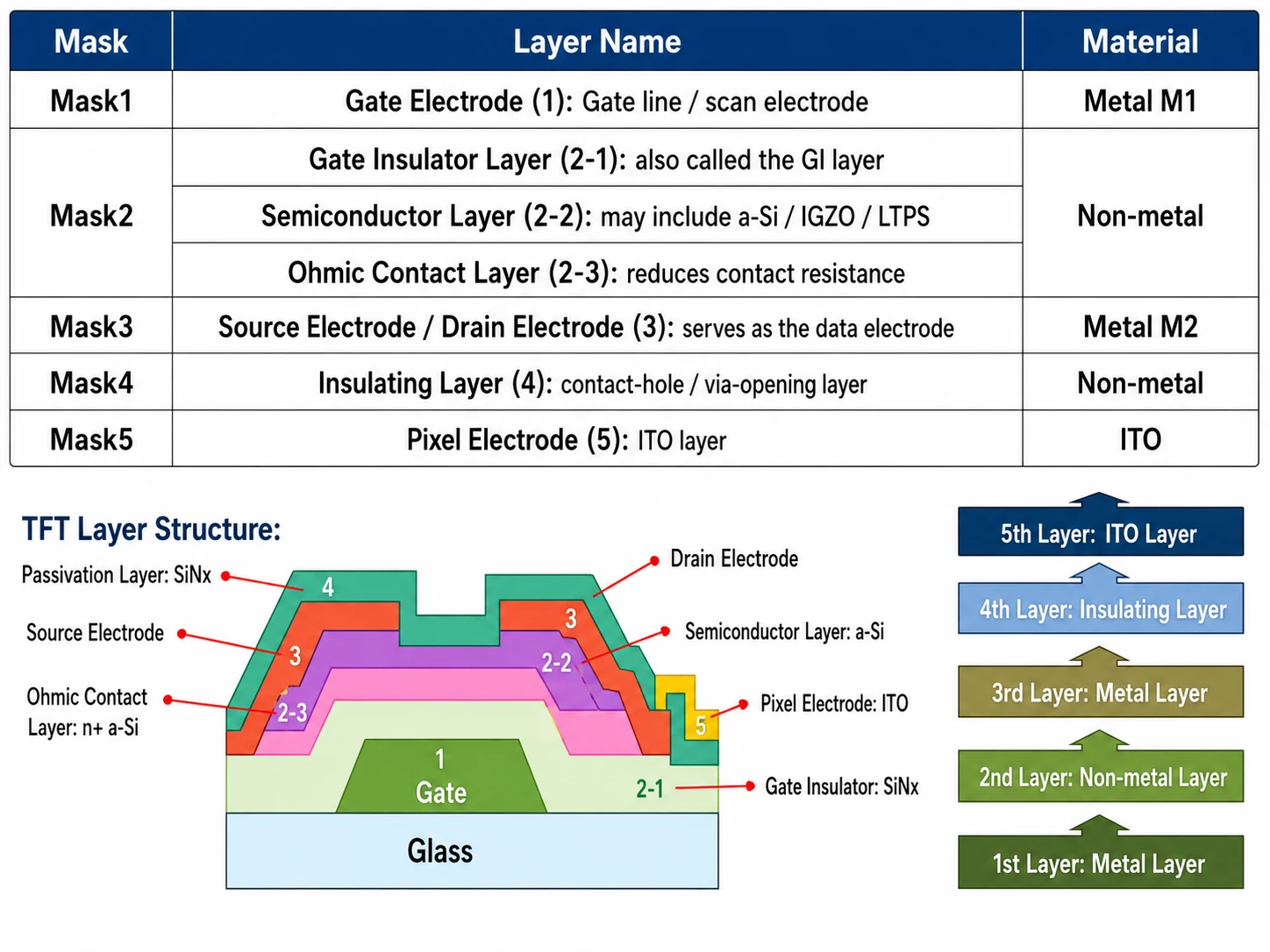
The 5-mask TFT process is an a-Si TFT-LCD array manufacturing flow that patterns five functional layer groups: gate metal, the active semiconductor stack, source/drain metal, passivation with contact vias, and the pixel ITO electrode.
- Each mask defines one functional layer group through coating, exposure, development, etching and photoresist removal.
- The five masks build the transistor, signal lines, protective layer and transparent pixel electrode on the array glass.
- Mask count is process-dependent; an IPS structure may add a common-electrode mask.
On this page
- Why the process starts from the TFT layer stack
- Mask 1: Gate electrode and scan line
- Mask 2: Gate insulator, semiconductor and ohmic contact
- Mask 3: Source, drain, data line and channel
- Mask 4: Passivation and contact via
- Mask 5: Pixel ITO electrode
- Five-mask process summary
- 5-mask versus 6-mask TFT processes
- Technical references
- Related TFT-LCD array guides
Why the process starts from the TFT layer stack
The array process is easier to understand when each lithography step is connected to the final TFT-LCD array substrate structure. In a typical TN-mode a-Si example, the substrate contains gate metal, gate insulator, semiconductor and ohmic-contact films, source/drain metal, passivation and the transparent pixel electrode.
Mask 1: Gate electrode and scan line
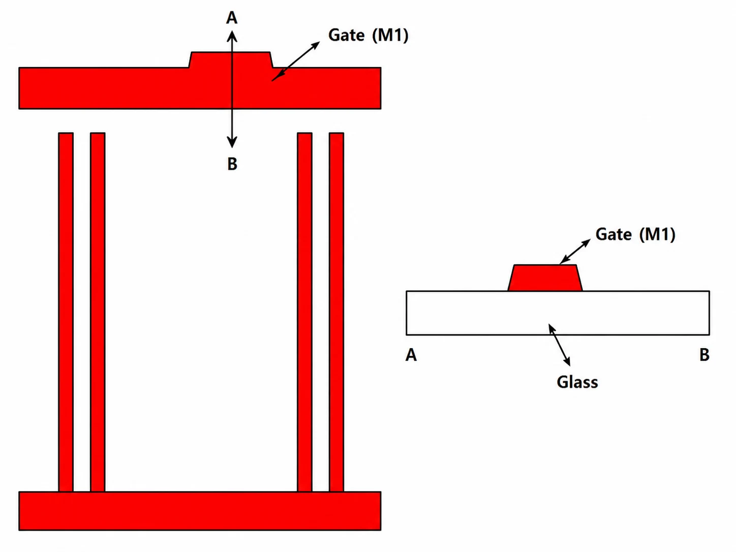
Mask 1 defines the gate electrode and horizontal scan line on the cleaned glass substrate. A representative sequence is metal deposition by PVD, photoresist coating, exposure and development, metal etching, and photoresist stripping. Film material and etching chemistry depend on the factory process.
Mask 2: Gate insulator, semiconductor and ohmic contact
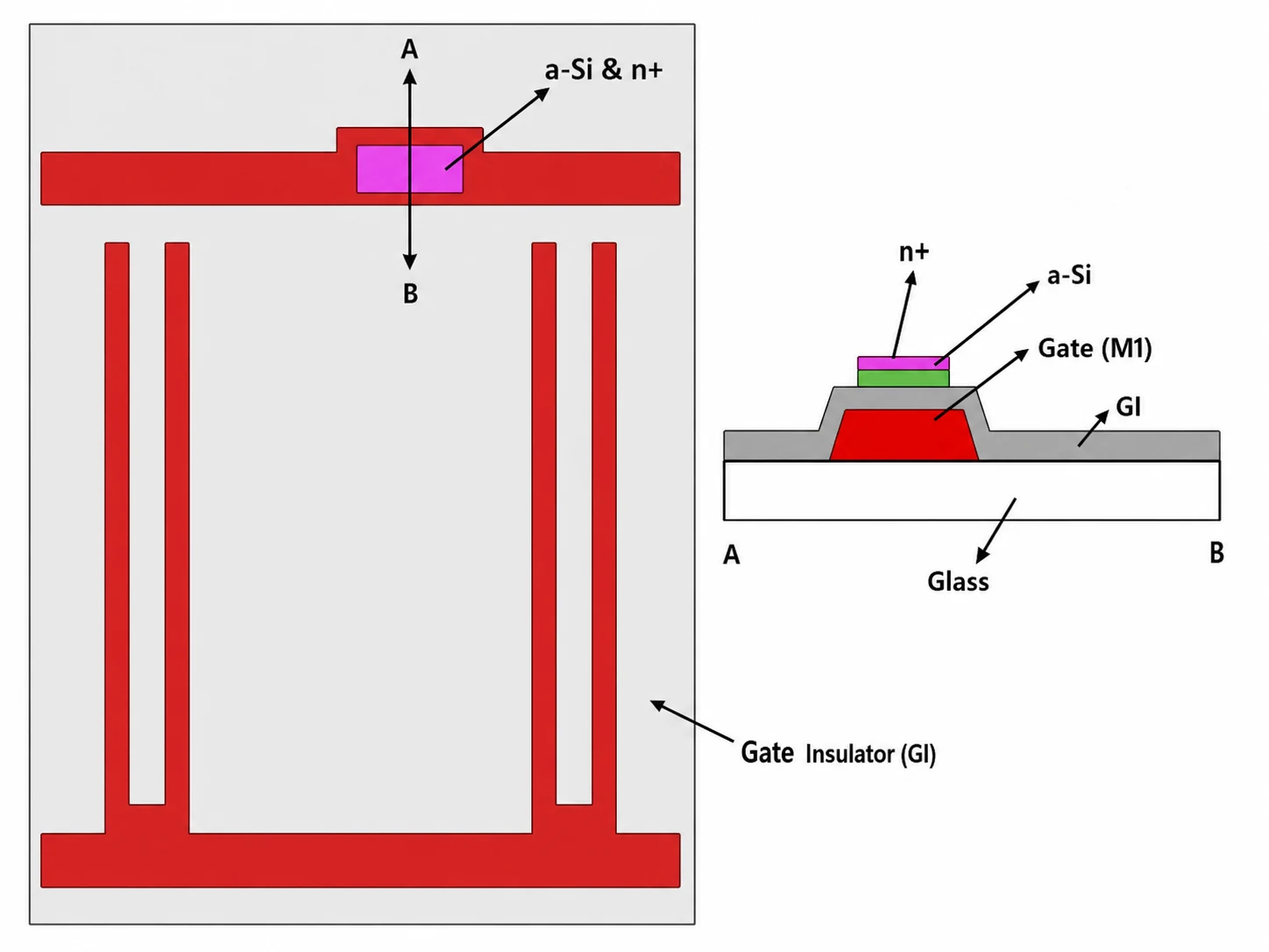
Mask 2 patterns the active stack above the gate. The gate insulator, intrinsic a-Si semiconductor and doped N+ a-Si ohmic-contact films are commonly deposited by CVD before lithography and dry etching define the active island. This stack electrically isolates the gate while creating the transistor channel and low-resistance contacts.
Mask 3: Source, drain, data line and channel
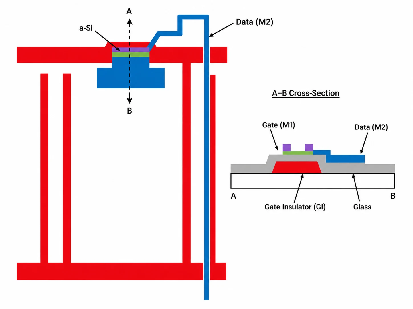
Mask 3 patterns the source/drain electrodes and vertical data line. After source/drain metal deposition and lithography, metal etching defines the electrodes. The exposed N+ a-Si between source and drain is then removed to open the channel while preserving the intrinsic semiconductor below.
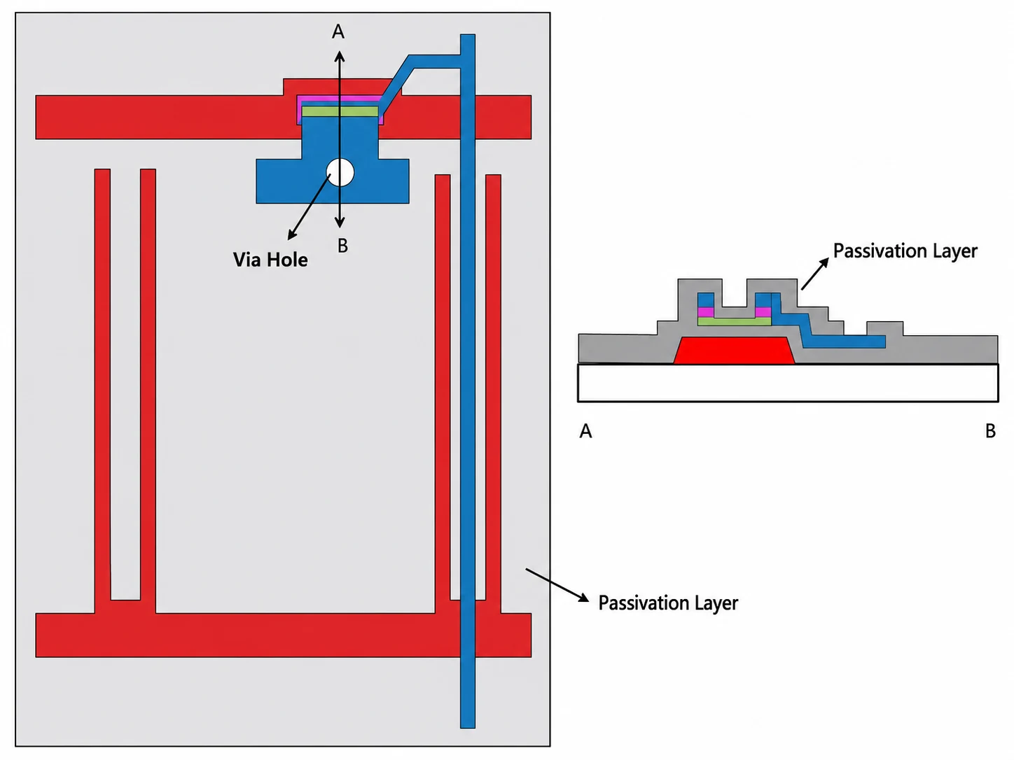
Mask 4: Passivation and contact via
Mask 4 defines openings in the passivation layer. Passivation protects the TFT and signal metal from the later process environment, while the contact via exposes the drain region needed to connect the pixel electrode. Via alignment and etch control are important for contact resistance and yield.
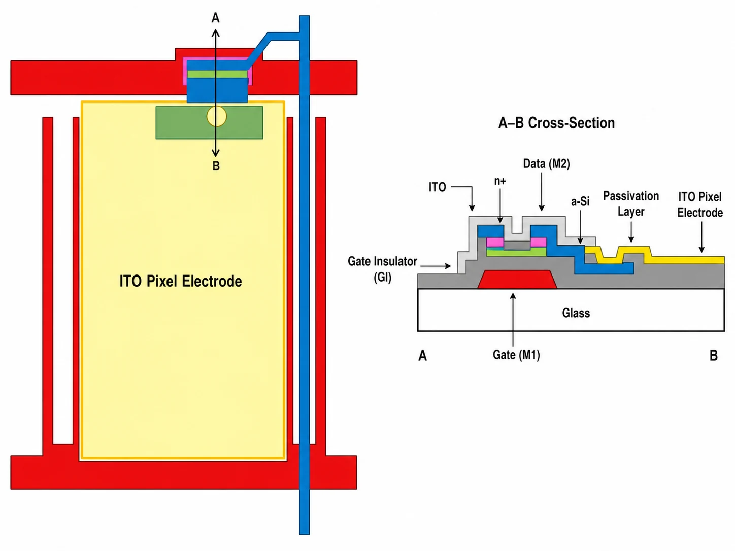
Mask 5: Pixel ITO electrode
Mask 5 patterns the transparent pixel electrode. ITO is deposited, coated with photoresist, exposed, developed and etched. The pixel electrode connects to the drain through the Mask 4 contact via, completing the five-mask TFT array substrate.
Five-mask process summary
| Mask | Primary layer group | Electrical purpose |
|---|---|---|
| 1 | Gate electrode and scan line | Controls transistor switching by row. |
| 2 | Gate insulator, semiconductor and ohmic contact | Forms the insulated active transistor stack. |
| 3 | Source/drain electrodes, data line and channel | Delivers the pixel signal and defines the TFT channel. |
| 4 | Passivation and contact via | Protects the TFT and exposes the drain contact. |
| 5 | Pixel ITO electrode | Applies the electric field that controls the pixel. |
5-mask versus 6-mask TFT processes
Five masks are not a universal rule for every TFT-LCD backplane. An IPS design can require an additional common-electrode pattern, while other process integrations may combine or separate layer steps differently. Materials, device architecture, reliability targets and factory capability determine the final mask count. For the shared patterning principles, see the TFT-LCD array photolithography guide.
Frequently asked questions
What is the 5-mask TFT process?
It is an a-Si TFT-LCD array flow that patterns five functional layer groups: gate metal, the active semiconductor stack, source/drain metal, passivation with contact vias, and pixel ITO.
Why can an IPS TFT-LCD require six masks?
An IPS structure can add a patterned common electrode, so it may require one more mask than a simpler five-mask TN example. The exact sequence depends on the backplane design and process integration.
Does each mask equal one deposited film?
No. One mask can pattern a group of films. In the five-mask example, Mask 2 covers the gate-insulator, semiconductor and ohmic-contact stack rather than only one film.
Is the five-mask array process the same at every factory?
No. The functional sequence is similar, but film materials, deposition methods, etching chemistry, dimensions and process controls vary by design and production line.
Technical references
- Applied Materials: Amorphous SiliconBackground on a-Si as an active-matrix TFT-LCD semiconductor.
- AGC: Glass Substrates for TFTsDisplay-glass requirements for TFT array fabrication.
- Nippon Electric Glass: Alkali-Free Glass SubstrateProperties of alkali-free glass used for TFT processes.
- SID / Wiley: Beyond Amorphous-Silicon TFTsMaterial and mobility context for TFT backplanes.
Related TFT-LCD array guides
- Complete TFT-LCD array manufacturing process
- TFT-LCD array substrate structure
- Positive and negative photoresist, exposure and etching
- Materials used in TFT-LCD array fabrication
- Copper versus aluminum gate electrodes
Need help selecting a TFT-LCD module?
Array process details explain how the panel is built; an OEM RFQ should translate them into module requirements such as size, resolution, interface, brightness, touch, environment and lifecycle.


