Optoelectronic Engineering Manual
7-Inch 1024×600 TFT-LCD Module: Architectural Integration Framework
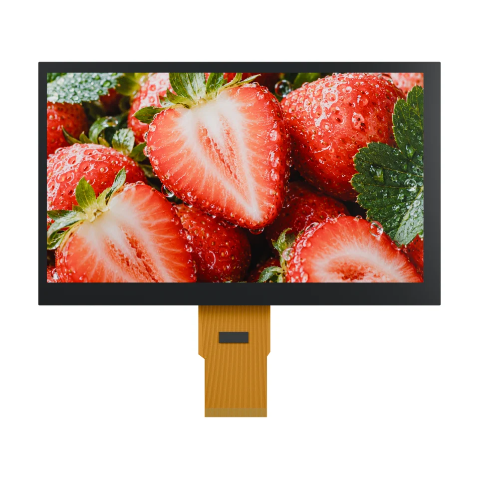
A 7-inch 1024×600 TFT LCD module is commonly used in industrial HMI, handheld terminals, medical devices, and compact control panels that need more UI space than 800×480 displays. Before RFQ, confirm the interface, brightness target, touch or cover lens, viewing angle, bonding method, operating temperature, and long-term supply plan.
Quick answer: when a 7-inch 1024×600 TFT LCD fits
Choose a 7-inch 1024×600 TFT LCD module when the device needs a compact screen with enough resolution for menus, charts, controls, and status data. The key decision is not only pixel count; the display stack must match the enclosure, interface, brightness, touch, and reliability requirements of the final product.
For an RFQ, prepare the active area or outline size, interface type, brightness target, operating temperature, touch or cover lens needs, optical bonding requirement, expected annual quantity, and lifecycle expectations.
Resolution & PPI Spatial Density Analysis
Transitioning a device interface from a baseline 800×480 array to a 1024×600 pixel matrix expands active layout area without modifying physical device packaging boundaries. The 1024×600 array hosts 614,400 active emission nodes—a 60% increase in layout capacity over 800×480 platforms.
GRID-REF: 7-INCH SPATIAL DATA PLATFORM ANALYSIS
| Parametric Variable | 800×480 Display Standard | 1024×600 Display Standard | Hardware Integration Impact |
|---|---|---|---|
| Active Pixel Matrix | 800 × 480 (WVGA) | 1024 × 600 (WSVGA) | 60% expansion in available UI layout block capacity. |
| Total Emitter Nodes | 384,000 sub-pixels | 614,400 sub-pixels | Enables parallel dashboard rendering and low-aliasing waveforms. |
| Spatial Resolution Density | Approx. 133 PPI | Approx. 170 PPI | Facilitates clear rendering of sharp, high-legibility 8-point fonts. |
| Interconnect Bus Load | Parallel RGB (Typical) | Single-Channel LVDS (Standard) | Reduces pin count while mitigating EMI/EMC radiation fields. |
| Timing Clock Frequency | ~33.3 MHz (Typical) | ~51.2 MHz (Typical) | Demands strict impedance matching and signal line layout verification. |
Industrial & Mission-Critical Application Mapping
Sourcing parameters change depending on the operational environment. The 7-inch 1024×600 platform serves as a standard visualization node across specialized B2B industries, with each deployment path following specific qualification workflows.
MATRIX-REF: INDUSTRY-SPECIFIC RELIABILITY PRIORITIES
| Deployment Field | Core Stress Variables | Optoelectronic Architecture Selection | Risk Controls To Execute |
|---|---|---|---|
| Industrial HMI Controls | 24/7 runtimes, transient voltage surges, high ambient electrical noise. | Single-channel LVDS + Thick-glove PCAP touch controller firmware. | Verify EMC margins, ground plane noise shielding, and loop isolation. |
| Medical Monitor Arrays | Chemical splash exposure, strict sanitization protocols, parallax visibility limits. | IPS full-view alignment + Chemically strengthened vacuum OCA bonding. | Verify chemical compatibility limits and contrast stability. |
| Precision Instrumentation | Zero-drift numeric tracking, continuous trace graphing, micro-step menus. | High-contrast stable timing cells with approx. 170 PPI density. | Verify clock tracking drift limits and font anti-aliasing. |
| Automotive Electronics | Thermal shock cycling, mechanical vibration spikes, solar loading. | Extended wide-temp fluid layers (-30°C to +85°C) + IATF 16949 documentation. | Execute full PPAP / APQP loops and verify L70 degradation slopes. |
For comprehensive sector-level validation methodologies, cross-reference our global LCD Display Application Case Studies.
Integration Topology: Bare Cells vs. Complete Modules
Engineering teams must verify sourcing boundaries before completing enclosure designs. Integrating a bare liquid crystal cell requires custom backlight engineering, optical sheet sorting, precision cleanroom alignment, and custom flexible printed circuit (FPC) design.
Conversely, a complete module assembly provides a turnkey system. It integrates backlighting arrays, mechanical bezel constraints, and tailored interconnect boundaries, mitigating system-level qualification risks.
Structural Layer Analysis
1. Chemically Strengthened Cover Glass Layer
Serves as the primary defensive barrier. Structural implementations specify chemical tempering to achieve high surface hardness, paired with tailored black border masking prints, anti-glare (AG) finishes to disrupt external light reflections, or anti-reflective (AR) multi-layer stacks.
2. Projected Capacitive (PCAP) Touch Matrix
Implements an isolated grid layout paired with high-performance controller ICs. Industrial applications require custom firmware configurations to sustain multi-touch tracking through 4mm safety glass covers, industrial fluid film exposure, or thick multi-layer gloves. Detailed integration options are compiled in our Touch & Cover Lens Engineering Directory.
3. Vacuum Optical Clear Adhesive (OCA) Stack up
An index-matched refraction matching medium completely filling the internal structural void between the cover glass and polarizers. Vacuum application cuts internal ambient light reflections below 0.5%, eliminates sub-glass moisture condensation risks, and increases structural impact force dissipation.
4. Wide-Viewing-Angle IPS Liquid Crystal Chemistry
Controls pixel-level switching behavior. IPS chemistry ensures full symmetric viewing angles, preventing contrast inversion or grayscale degradation when the display module is viewed from off-center operator positions.
5. LED Backlight Array & L70 Life Tracking
Dictates the absolute useful lifetime of the node. Backlight lifecycles are defined strictly by the L70 degradation parameter—the runtime point where peak luminance output decays to exactly 70% of initial calibrated values under nominal driving currents and maximum junction temperature constraints.
6. Interconnect Interface Bus Alignment
Single-channel low-voltage differential signaling (LVDS) is the standard interconnect architecture for this 1024×600 profile. LVDS converts wide high-frequency single-ended CMOS data lines into tightly matched differential pairs, optimizing signal integrity while suppressing EMI generation. For interface risk profiling, review the MIPI vs LVDS vs RGB LCD Interface Comparison Guide.
Engineering Selection Self-Test
Run your hardware profile through this diagnostic sequence before locking in component selection:
- [TEST 01] Does your GUI display real-time medical curves or sub-10pt technical text font sets? If confirmed, a 1024×600 array is necessary to prevent anti-aliasing errors.
- [TEST 02] Is your system architecture positioned adjacent to high-power inductive components? If confirmed, specify a single-channel LVDS interconnect with an integrated EMC ground plane shield.
- [TEST 03] Will the target device operate under direct sunlight or across unconditioned environments? If confirmed, require cleanroom vacuum OCA optical bonding to eliminate sub-glass fogging risks.
- [TEST 04] Is your end-product line tracking a multi-year manufacturing lifecycle footprint? If confirmed, require strict, contractually locked PCN / ECN and long-term supply guarantees before signing sample releases.
Verification Criteria Matrix
This checklist acts as the primary hardware review matrix for verifying technical parameters prior to engineering sample sign-off and enclosure tooling releases.
CHECKLIST-REF: TIER-1 COMPONENT AUDIT CRITERIA
| Parametric Group | Audit Focus Areas | B2B Sourcing Importance | Integration Risk Factors |
|---|---|---|---|
| Pixel Layout Data | 1024×600 array boundaries, active centering fields. | Defines graphic data limits within fixed mechanical footprints. | GUI text overlapping, frame truncation bugs. |
| Interconnect Routing | LVDS mapping formats, differential pair track lengths, pinouts. | Locks in interface signal matching with the host processor. | Unstable color map values, timing skew, noise flicker. |
| Illumination Profile | Calibrated nit output, drive current paths, L70 decay tracking. | Matches display performance to ambient environment limits. | Thermal junction overload, rapid luminance loss. |
| Touch Interface | PCAP matrix lines, I2C/USB controller registers, glove parameters. | Establishes tracking reliability across extreme conditions. | False input registrations, complete capacitive dropouts. |
| Mechanical Envelope | Bezel positioning coordinates, FPC bend radius limits, thickness tolerances. | Coordinates physical package interface boundaries. | Uneven enclosure pinch-points, mura pressure defects. |
| Procurement Lifecycles | MES tracking availability, PCN/ECN locking, EOL mitigation paths. | Guarantees continuous line access over production horizons. | Sudden line stops, forced PCB redesign costs. |
For specific technical customization requirements, review our dedicated Custom Engineering Platform Matrix.
Technical Q&A: Architectural Verification
Why is the 1024×600 pixel array critical for industrial upgrades?
The 1024×600 WSVGA matrix yields a high pixel density of approximately 170 PPI, expanding active UI layout real estate by 60% compared to legacy 800×480 WVGA displays. This density allows engineers to display small 8-point data labels, fine real-time curves, and dense parameter control panels without moving to a larger display size.
How does the single-channel LVDS bus reduce EMC propagation risk?
Unlike standard single-ended CMOS/TTL parallel RGB routing layouts that utilize up to 24 data lines cycling at high speeds, single-channel LVDS serializes data onto a small number of low-voltage differential signal pairs. This balanced differential transmission system naturally cancels out electromagnetic radiation patterns, helping the system pass strict industrial EMC validations.
What parameters are audited to prevent unexpected display component EOL situations?
Our manufacturing operations in Dongguan and Hubei implement long-term component lifecycle controls. Sourcing teams enforce a strict BOM-Lock phase, execute formal PCN / ECN protocols minimums of 90 days before raw component change implementations, and maintain 1:1 hardware cross-reference replacement paths to guarantee stable production-line continuity.
Request Optoelectronic Validation Review
Provide your display configuration data, required interface bus specifications, and expected environmental profiles. Success Intelligence provides complete technical validation reporting—including interface timing analysis, enclosure tolerance cross-checks, and lifecycle risk evaluations—prior to initial tooling and sample release.
Need help choosing or customizing an LCD module?
Share your target size, interface, brightness, touch panel, cover lens, operating temperature and annual quantity. Our engineering team can review the requirements and suggest a practical TFT, mono LCD or custom display path.
- Review TFT, mono LCD, touch panel and optical bonding options.
- Check interface, backlight, FPC, lifecycle and reliability requirements.
- Prepare a clearer RFQ so the quotation is faster and more accurate.
- Send LCD RFQUse RFQ Checklist
7-Inch 1024×600 TFT LCD Integration Readiness Check
A 7-inch 1024×600 TFT LCD is often a practical HMI size, but the buying decision should confirm more than diagonal size and resolution. Before sampling, check interface, enclosure, brightness, touch stack, viewing distance and production lifecycle together.
| Decision area | What to confirm | Why it matters |
|---|---|---|
| Resolution and UI density | 1024×600 layout, font size, icon density and operator viewing distance. | A good PPI number still fails if the real UI is crowded or viewed from too far away. |
| Interface path | RGB, LVDS, MIPI or controller-board approach. | The interface decides host processor fit, FPC design, cable length and bring-up risk. |
| Brightness and readability | Indoor, high brightness or sunlight-readable requirement. | Backlight, cover lens, bonding and heat should be reviewed before approving samples. |
| Touch and cover lens | PCAP/RTP, cover glass thickness, logo printing, AG/AR/AF and bonding. | The front stack changes mechanics, readability, touch response and durability. |
| Mechanical integration | Outline, active area, mounting method, FPC direction and connector position. | Mechanical mismatch can force redesign even if electrical specs look correct. |
When a 7-Inch TFT Module Is a Good Fit
Good fit signals
- The UI needs more room than a small handheld display but not a large panel.
- The enclosure can support a 7-inch active area and cover lens stack.
- The host can support the required interface and pixel bandwidth.
- The project needs HMI-style readability, touch and stable supply review.
RFQ files to send
- Mechanical drawing or enclosure opening.
- Preferred interface and host processor details.
- Brightness, touch, cover lens and operating temperature target.
- Sample quantity, annual forecast and lifecycle expectation.
7-Inch TFT Module FAQ
Is 1024×600 always better than 800×480 for a 7-inch HMI?
Not always. Higher resolution can improve UI detail, but it may increase bandwidth, firmware workload and interface requirements. Choose by real UI task, processor capability and product cost target.
What page should I review next?
For interface choice, review the TFT LCD interface guide. For custom structure, review custom TFT LCD modules.
Continue your LCD module engineering review
Use these technical guides to compare interface, optical bonding, sourcing risk, replacement planning and custom LCD project decisions before sending an RFQ.
Related technical guides
RFQ details to prepare
- Display size and resolution
- Interface, voltage and backlight target
- Brightness, touch panel or cover lens needs
- Operating temperature, quantity and application environment